1.5 MAX 10 Devices I/O Resources Per Package
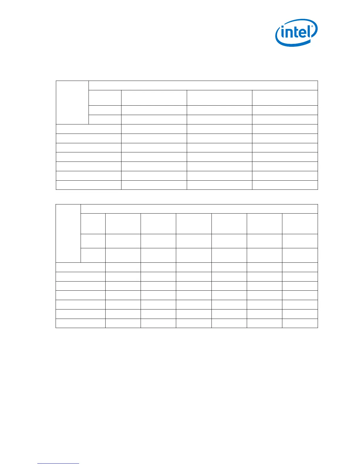
Table 5. Package Plan for MAX 10 Single Power Supply Devices
Device Package
Type M153
153-pin MBGA
U169
169-pin UBGA
E144
144-pin EQFP
Size 8 mm × 8 mm 11 mm × 11 mm 22 mm × 22 mm
Ball Pitch 0.5 mm 0.8 mm 0.5 mm
10M02 112 130 101
10M04 112 130 101
10M08 112 130 101
10M16 — 130 101
10M25 — — 101
10M40 — — 101
10M50 — — 101
Table 6. Package Plan for MAX 10 Dual Power Supply Devices
Device Package
Type V36
36-pin
WLCSP
V81
81-pin
WLCSP
U324
324-pin
UBGA
F256
256-pin
FBGA
F484
484-pin
FBGA
F672
672-pin
FBGA
Size 3 mm × 3
mm
4 mm × 4
mm
15 mm × 15
mm
17 mm × 17
mm
23 mm × 23
mm
27 mm × 27
mm
Ball
Pitch
0.4 mm 0.4 mm 0.8 mm 1.0 mm 1.0 mm 1.0 mm
10M02 27 — 160 — — —
10M04 — — 246 178 — —
10M08 — 56 246 178 250 —
10M16 — — 246 178 320 —
10M25 — — — 178 360 —
10M40 — — — 178 360 500
10M50 — — — 178 360 500
Related Links
• MAX 10 General Purpose I/O User Guide
• MAX 10 High-Speed LVDS I/O User Guide
1.6 MAX 10 Vertical Migration Support
Vertical migration supports the migration of your design to other MAX 10 devices of
different densities in the same package with similar I/O and ADC resources.
1 MAX
®
10 FPGA Device Overview
MAX 10 FPGA Device Overview
7