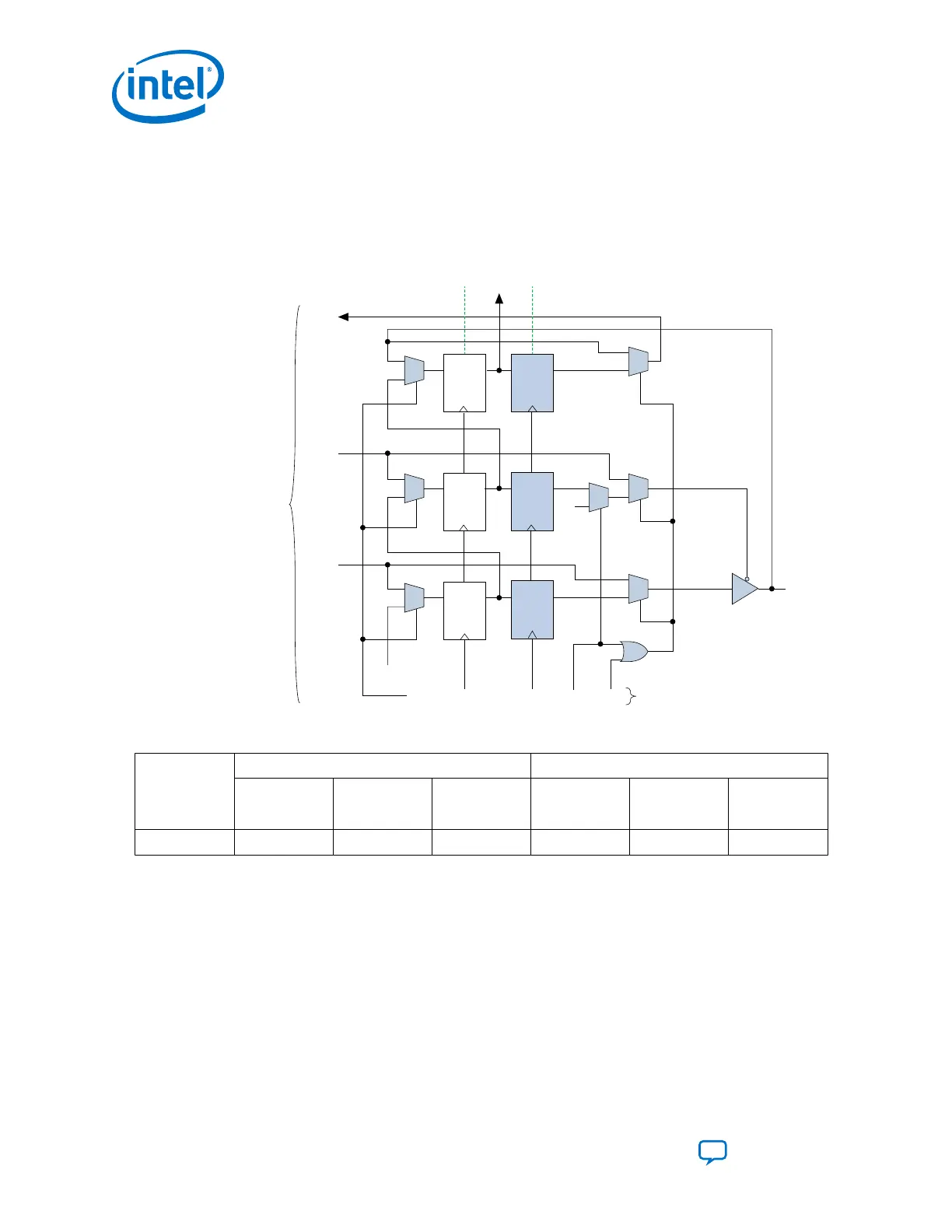
Figure 2. User I/O BSC with JTAG BST Circuitry for Intel MAX 10 Devices
The TAP controller generates the global control signals internally for the JTAG BST registers, shift, clock,
and update. The instruction register generates the MODE signal.
The data signal path for the boundary-scan register runs from the serial data in (SDI) signal to the serial data
out (SDO) signal. The scan register begins at the TDI pin and ends at the TDO pin of the device.
0
1
OUTPUT
OE
INPUTINPUT
OUTPUT
OE
From or
to Device
I/O Cell
Circuitry or
Logic Array
0
1
0
1
0
1
0
1
0
1
0
1
PIN_OUT
INJ
OEJ
OUTJ
VCC
SDO
Pin
SHIFT
SDI
CLOCK HIGHZ MODE
PIN_OE
PIN_IN
Output
Buffer
Capture
Registers
Update
Registers
Global
Signals
UPDATE
D Q
D Q
D Q D Q
D Q
D Q
Table 2. BSC Capture and Update Register for Intel MAX 10 Devices
Pin Type Captures Drives
Output
Capture
Register
OE Capture
Register
Input Capture
Register
Output Update
Register
OE Update
Register
Input Update
Register
User I/O
OUTJ OEJ PIN_IN PIN_OUT PIN_OE INJ
Note:
All VCC and GND pin types do not have BSCs.
2. JTAG BST Architecture
UG-M10JTAG | 2019.05.10
Intel
®
MAX
®
10 JTAG Boundary-Scan Testing User Guide
Send Feedback
6