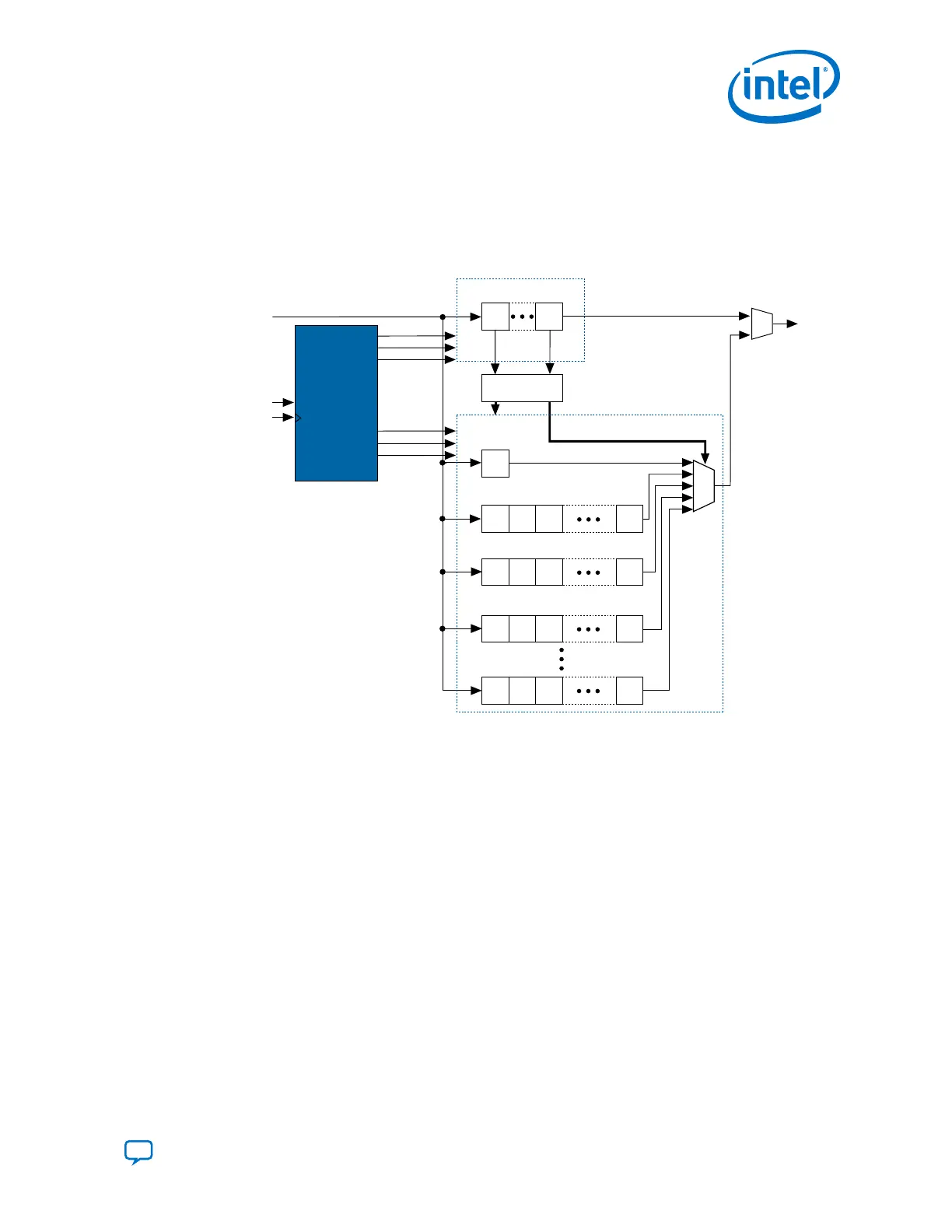
Figure 1. JTAG Circuitry Functional Model
• Test access port (TAP) controller—controls the JTAG BST.
•
TMS and TCK pins—operate the TAP controller.
•
TDI and TDO pins—provide the serial path for the data registers.
•
The TDI pin also provides data to the instruction register to generate the control logic for the data
registers.
a
UPDATEIR
CLOCKIR
SHIFTIR
UPDATEDR
CLOCKDR
SHIFTDR
TDI
Instruction Register
Bypass Register
Boundary-Scan Register
Instruction Decode
TMS
TCK
TAP
Controller
ISP Registers
TDO
Data Registers
Device ID Register
2.3. JTAG Boundary-Scan Register
You can use the boundary-scan register to test external pin connections or to capture
internal data. The boundary-scan register is a large serial shift register that uses the
TDI pin as an input and the TDO pin as an output. The boundary-scan register consists
of 3-bit peripheral elements that are associated with Intel MAX 10 I/O pins.
2.3.1. Boundary-Scan Cells in Intel MAX 10 I/O Pin
The Intel MAX 10 3-bit BSC contains the following registers:
•
Capture registers—connect to internal device data through OUTJ, OEJ, and
PIN_IN signals.
•
Update registers—connect to external data through PIN_OUT and PIN_OE signals.
2. JTAG BST Architecture
UG-M10JTAG | 2019.05.10
Send Feedback
Intel
®
MAX
®
10 JTAG Boundary-Scan Testing User Guide
5