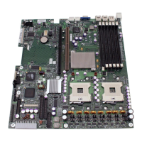
Intel® Server Board SE7520JR2 Connectors and Jumper Blocks
Revision 1.0
C78844-002
185
FMC Signal Name FMC
Pin
Description
FML_SINTEX 27 Fast Management Link Slave Interrupt/Clock Extension. This signal is driven by
the FML Slave, and has a dual usage:
Used as an Alert signal for the slave to notify master that data is ready to be
read from slave
Used as a clock Extension (Stretching) for the slave to indicate to the master to
extend its low period of the clock
FML_MDA_I2CSDA 28 Fast Management Link Data Out. This signal is driven by the FML Master.
When not configured as FML, this signal is used as I2C data
ICH_LCLK 31 LPC 33Mhz clock input
USB_M 32 Reserved for future use as USB input. Baseboard can leave as NC
FMM_SYSIRQ 33 KCS interrupt signal from FMM Card.
USB_P 34 Reserved for future use as USB input. Baseboard can leave as NC
ICH_LAD1 35 LPC Address/data bus Bit 1
FMM_RSMRST_N 36 When this signal is asserted, the FMM is held in reset. This is a Standby reset
indication, and should be driven by a Standby monitor device such as the
Heceta7 or Dallas DS1815
ICH_LFRAME_N 37 LPC Cycle Framing
ICH_LAD0 38 LPC Address/data bus Bit 0
ICH_LAD3 39 LPC Address/data bus Bit 3
ICH_LPCPD_N 40 LPC Power down indication
ICH_LAD2 41 LPC Address/data bus Bit 2
FMM_LPCRST_N 40 LPC bus reset. Must be properly buffered on motherboard to ensure
monotonicity
DFP_CLK 46 Serial clock signal for DFP EDID device. Must connect to DFP_CLK pin on the
graphics chip.
DFP_DAT 48 Serial data signal for DFP EDID device. Must connect to DFP_DAT pin on the
Graphics chip.
IPMB_I2C_5VSB_SDA 49 Connects to IPMB header
IPMB_I2C_5VSB_SCL 50 Connects to IPMB header
SMB_I2C_3VSB_SDA 51 This bus should connect to the PCI slots, ICH, and mBMC (host I/F). An
isolated version of this bus (non-Standby) should connect to the DIMMs, and
clock buffer(s)
SMB_I2C_3VSB_SCL 52 This bus should connect to the PCI slots, ICH, and mBMC (host I/F). An
isolated version of this bus (non-Standby) should connect to the DIMMs, and
clock buffer(s)
PERIPH_I2C_3VSB_SDA 53 This bus should connect to the mBMC (Peripheral I/F), SIO, Heceta, Front panel
header. A level shifted version of this bus (5V Standby) should connect to the
Power Supply header
PERIPH_I2C_3VSB_SCL 54 This bus should connect to the mBMC (Peripheral I/F), SIO, Heceta, Front panel
header. A level shifted version of this bus (5V Standby) should connect to the
Power Supply header
MCH_I2C_3V_SDA 55 This bus should connect to the Northbridge and I/O bridge (MCH and PXH
respectively in the LH chipset). In a system that supports PCI Hot Plug, this bus
should also connect to the Power control devices if possible (such as the
MIC2591 for PCI-Express for example)
MCH_I2C_3V_SCL 56 This bus should connect to the Northbridge and I/O bridge (MCH and PXH
respectively in the LH chipset). In a system that supports PCI Hot Plug, this bus
should also connect to the Power control devices if possible (such as the
MIC2591 for PCI-Express for example)
LAN_I2C_3VSB_SDA 57 LAN usage
 Loading...


