Boot ROM inbuilt Menu, self tests, setups, etc 5 - 3
Revision 1 - 07 July
1999 Event 4 TECHNICAL MANUAL
Move 80 to 20000003 IC11 pin 29 Write to FLASH byte 3
Move 20000004 to
CPU
IC11-14 pin 24 Read from FLASH
Move AA to 606A0000 IC65 pin 13 PC Memory Write
Move 606A0000 to
CPU
IC65 pin 14 PC Memory Read
Move 55 to 60000000 IC65 pin 50 PC IO Write
Move 60000000 to
CPU
IC65 pin 49 PC IO Read
Table 3: Bus exercise event summary
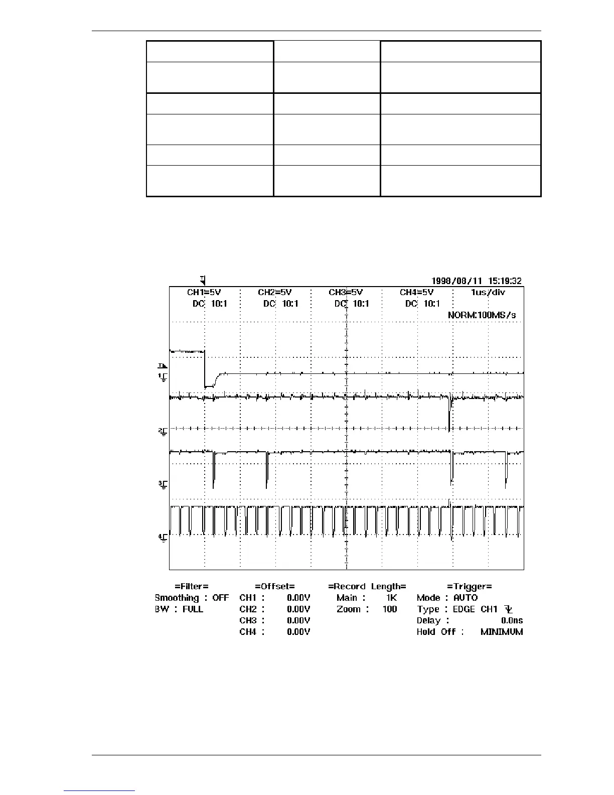
Figure 1 shows the relationship between L5, IC16 WR, and the CPU DACK signals as
measured while running this test.
Figure 1: Sample waveform during Bus Exercise
Trace #1: L5
Trace #2: IC16 Pin 29 (WR)
Trace #3: IC1 pin 44 (DACK1)
Trace #4: IC1 pin 43 (DACK0)
 Loading...