
EasyManuals Logo

JBL FLIP 3 Service Manual

JBL FLIP 3
30 pages
To Next Page IconTo Next Page
To Previous Page IconTo Previous Page
Page #21 background imageLoading...
Page #21 background image
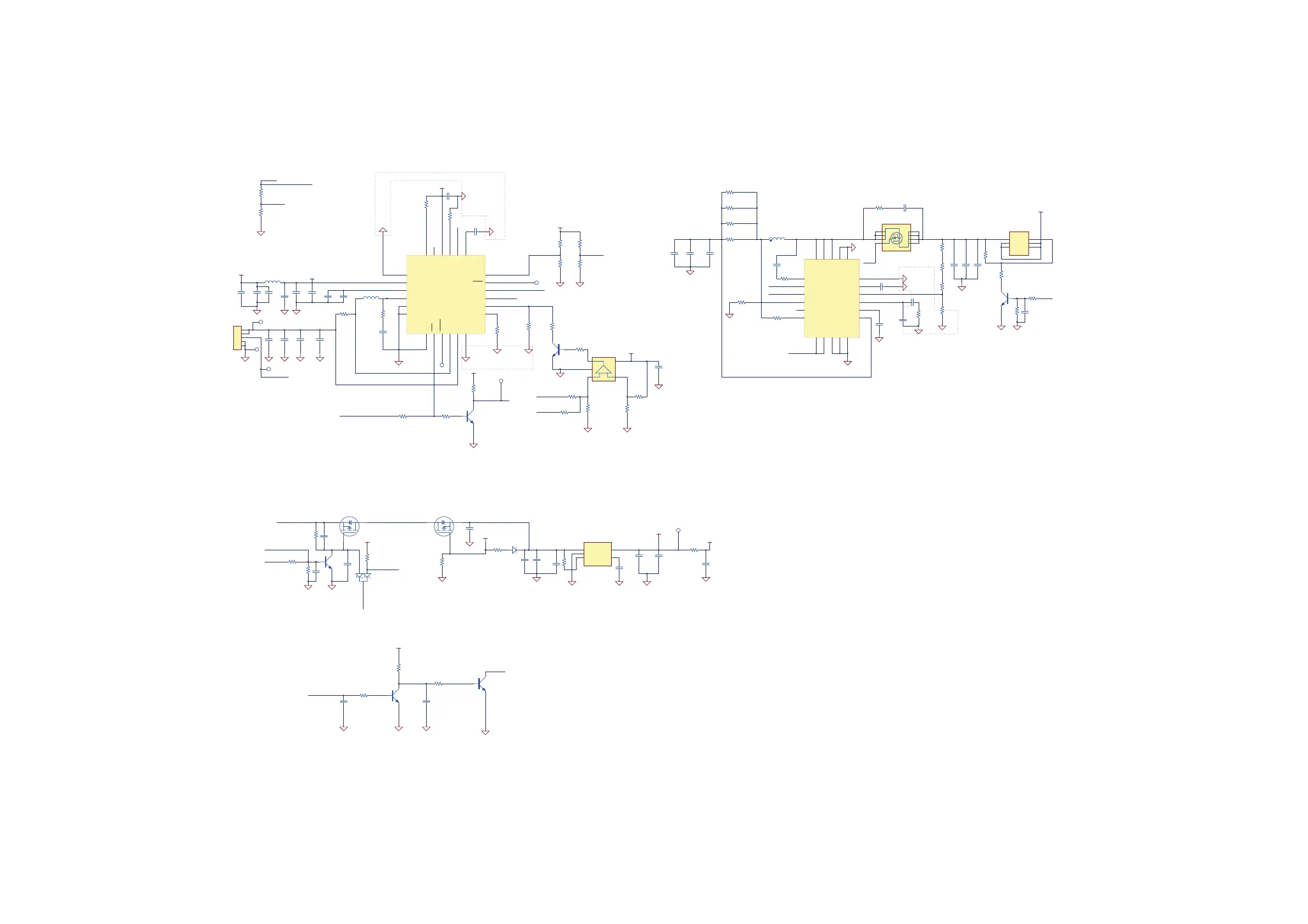
Main Board Circuit Diagram:
7-7
N/C
1
CHG
2
BOOST
3
CSP
4
BATT
5
AGND
6
OLIM
7
ISET
8
NTC
9
FB
10
ACOK
11
REG
12
TMR
13
PWIN
14
ILIM
15
VCC
16
VB
17
EN
18
MODE
19
VIN
20
SYS
21
SW
22
PGND
23
PGND
24
U9
MP2637
BST
1
SDR
2
OUT
3
EN
4
MODE
5
SENSE
6
SW
7
SW
8
PGND
9
PGND
10
IN
11
VDD
12
COMP
13
FB
14
SS
15
AGND
16
PGND
17
PGND
18
SW
19
SW
20
SW
21
PGND
22
U7
MP9428
USB+5V
charge_in_5V
charge_in_5V
AGND AGND
PWIN
PWIN
AGND
Charge_in_EN
AGND
charge_in_VCC
5%
0805
R407
0.02 ohm
NTC
NTC
AGND
charge2_sys_5V
AGND
NTC
charge2_sys_5V
AGND
AGND AGND
charge_sys_FB
/ACOK
/BOOST
R501
0.01ohm
R502
0.01ohm
R503
0.01ohm
R504
0.01ohm
C501
22uF 25V
AGND
C502
22uF 25V
C503
22uF 25V
VBAT_1
VBAT_1
2.2uF
C504
AGND
Boost_10V
AGND
SDR
VOUT
1
V-
2
VIN+
3
VIN-
4
V+
5
-+
U8
NC
USB+5V
AGND
AGNDAGND
USB_D+
1
32
Q4
NC
AGND
USB_D-
C414
22UF
C415
22UF
10V
C407
22UF
C406
22UF
25V
C508
22UF
25V
C509
22UF 25V
C510
22UF
3428_SW
3428_SW
different pair
same length
S
1
F
2
L501
1.5UH, 15A
2.2ohm
R516
1nF
C511
5%
0805
R441
NC
NC
C416
AGND
AGND
AGND
AGND
AGND
AGND
AGNDAGNDAGNDAGNDAGND
AGNDAGNDAGND
AGND
1
2
3
4
5
J401
C400
100NF
C426
100nF
C409
100NF
1K
R404
15K
R414
C404
100nF
C410
330nF
15K
1%
R400
5.1k
1%
R401
21.5K
1%
R410
5.1k
1%
R411
NC
R425
68K
1%
R421
51k
R420
NC
R431
C423
NC
R426
Nc
R427
nc
R429
NC
NC
R428
NC
R437
TP400
TP401
100K
R432
1%
R423
5.36k
1%
R424
15k
100K
R506
0 OHM
R510
C507
100nF
220k
R512
34k
R509
51
R511
Boost_10V
Boost_EN
AGND
D
6
D
5
S
4
G
3
D
2
D
1
Q2
MTP2603
100K
R508
1K
R515
1
32
Q3
MMBT3904
AGND
47K
R505
100K
R514
AGND
24K
R513
1
32
Q5
MTP3401N3
VBAT_1
100k
1%
R433
1
32
Q7
MMBT3904
AGND
C427
100nF
100k
1%
R435
AGND
47k
1%
R434
Deep_Sleep
2
3
1
D401
BAT54C
PW_K E Y
100K
R436
VCC_switch_3V3
SW_POWER
C402
NC
Hand_Reset
4.7K
R442
AGND
USB+5V
AGND
AGND
10K
R419
AGND
10V
C420
10UF 10V
C412
10UF
5.1
R430
AGND
VCC_audio_3V3
VCC_switch_3V3
33k
R439
1
32
Q408
MMBT3904
100k
5%
R438
AGNDAGND
BT_reset_in
1k
5%
R440
AGND
1
32
Q407
MMBT3904
AGND
Hand_Reset
VCC_AMP_10V
G
4
S
3
S
2
S
1
D
5
D
6
D
7
D
8
Q1 MTB04N03
10V
C428
4.7uF
OUT
5
BP/FB
4
EN
3
GND
2
IN
1
U5
SD35
AGND
C159
1.5nF
AGND
VCC_switch_3V3
100K
R173
10K
R172
VCC_switch_3V3
CHARGE_in_STATU(/CHG)
AGND
1
32
Q21
MMBT3904
C408
1uF
C421
1uF
C422
1uF
C424
1uF
C425
1uF
C403
100NF
C417
100NF
C418
100NF
1uF
C405
C419
1NF
C506 2.2nF
C429
10NF
C505
33NF
charge2_sys_5V
C512
10NF
1 2
L401
CKCD5D28-2.2ȝH/N
200 OHM
R517
1
3 2
Q6
MTP3401N3
SDR
L402
100 @ 100MHz
D403
1N4148WS
15k
R507
TP1
TP2
TP3
0603
5%
R443
10 ohm
TP48
TP49
6.3V
C401
22UF
6.3V
C430
22UF

Other manuals for JBL FLIP 3

Questions and Answers:

Question and Answer IconNeed help?

Do you have a question about the JBL FLIP 3 and is the answer not in the manual?

JBL FLIP 3 Specifications

General IconGeneral
Speaker type-
Driver diameter40 mm
Number of drivers2
Number of speakers1
Audio output channels- channels
Impedance- Ω
Frequency range85 - 20000 Hz
RMS rated power16 W
Signal-to-Noise Ratio (SNR)80 dB
Bluetooth version4.1
USB charging portYes
Bluetooth profilesA2DP, AVRCP, HFP, HSP
USB connector typeMicro-USB
USB 2.0 ports quantityUSB 2.0 ports have a data transmission speed of 480 Mbps, and are backwards compatible with USB 1.1 ports. You can connect all kinds of peripheral devices to them.
Connectivity technologyWireless
Battery voltage3.7 V
Battery capacity3000 mAh
Power source typeBattery
Battery life (max)10 h
Battery recharge time3.5 h
Product colorTurquoise
Protection featuresSplash proof
Recommended usageUniversal
Quantity per pack1 pc(s)
Weight and Dimensions IconWeight and Dimensions
Depth64 mm
Width169 mm
Weight450 g

Related product manuals