37
Dolby Pro-Logic
Ò
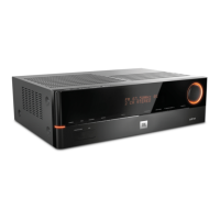
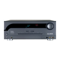
A/V Receiver JSR-400
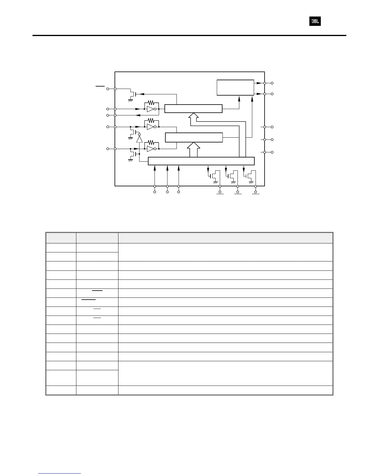
INTEGRATED CIRCUIT DIAGRAMS 2
2
1
11
6
11
14
15
12
13
12
XIN
XOUT
FMIN
AMIN
PD1
PD2
VDD1
VDD2
VSS
SYC
345
789
CE CL DATA
BO1 BO2 BO3
6
Shift Register - Latch
Programable Divider
Reference Divider
Phase Detector
Charge Pump
Tuner PCB IC2 - (LM7001)
(PLL Synthesizer and Controller)
Terminal Description
Pin No. Terminal Description
1
XOUT
Connect to the 7.2 Mhz crystal oscillator.
2
XIN
3
CE
Chip enable terminal. Connect to the PLL terminal of microprocessor.
4
5CL
Serial clock input terminal. Connect to the CLOCK terminal of microprocessor.
5
DATA
Serial data input. Connect to the DATA terminal of micro processor.
6
SYN
Not used
7
AUTO/MONO
AUTO/MONO selection output terminal. “L” when FM.
8
FM
FM band control output terminal. “L” when FM.
9
AM
AM band control output terminal. “L” when AM.
10
AMIN
AM local oscillator input terminal.
11
FMIN
FM local oscillator terminal.
12
V
DD
1
Power supply terminal for back-up.
13
V
DD
2
Power supply terminal.
14
PD1
Charge pump output of the phase detector which constitues the PLL. High level is output when the divided
local oscillator frequency is higher than the reference frequency. In the opposite case, low level is output.
Floating occurs when the frequency matched. The output is applied to the variable capacitor diode in the
local oscillator through the low pass filters.
15
PD2
16
V
SS
Ground terminal.