CH-X400/CH-X450
1-32
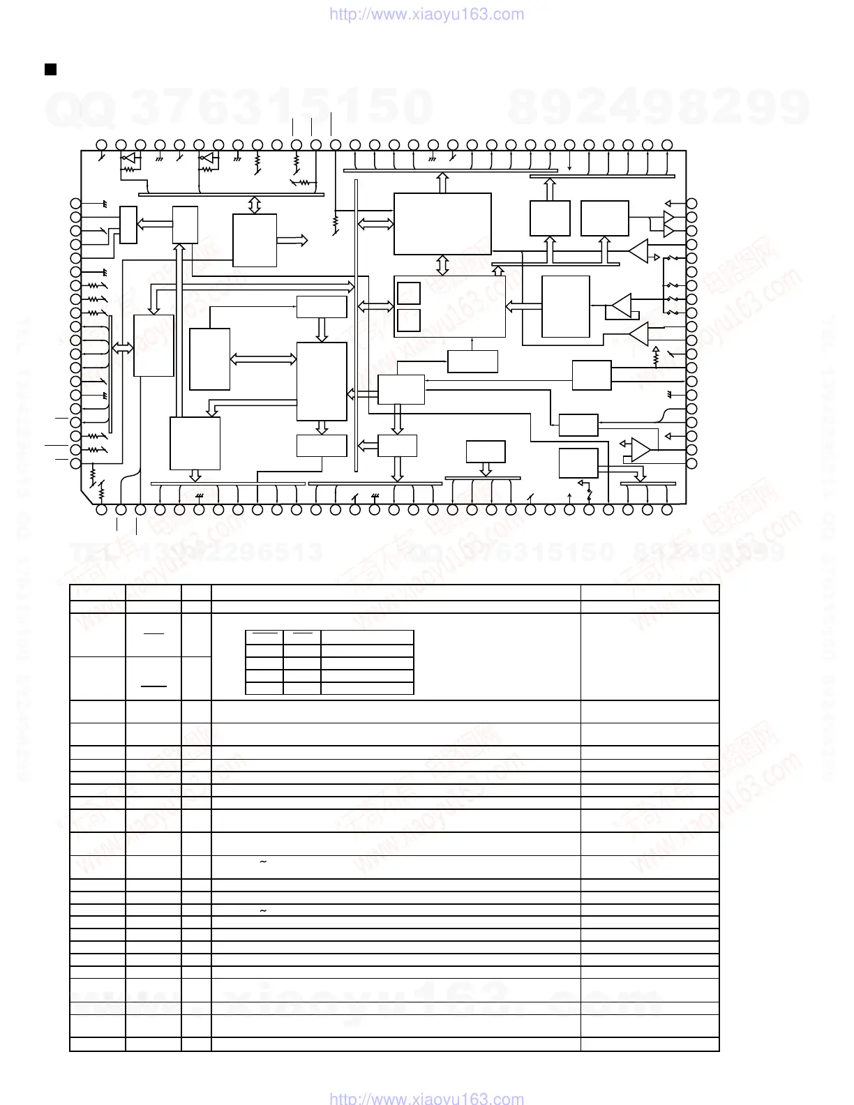
2.Pin function
50 V
REF
49 TRO
48 FOO
47
TEZI
46 TEI
45 TSIN
44 SBAD
43 FEI
42 RFRP
41 RFZI
40 RFCT
39 AV
DD
38 RFI
37 SLCO
36 AV
SS
35 VCOF
34 VCOREF
33 PV
REF
32 LPFO
31 LPFN
81DV
SR
1 2 3
4 5
6
7 8 9 10 11 12 13
14 15
16 17 18 19 20 21 22
23 24 25
26
27 28
TEST0
HSO
UHSO
EMPH
LRCK
V
SS
BCK
AOUT
DOUT
MBOV
IPF
SBOK
CLCK
V
DD
V
SS
DATA
SFSY
SBSY
SPCK
SPDA
COFS
MONIT
V
DD
TESIO0
P2V
REF
HSSW
ZDET
PDO
29
TMAXS
30
TMAX
80
XV
DD
79
XO
78
XI
77
XV
SS
76
V
DD
75
PXO
74
PXI
73
V
SS
72
TESIO1
71
TESIN
67
IO3
66
IO2
65
IO1
64
IO0
63
V
SS
62
V
DD
61
FLGD
60
FLGC
59
FLGB
58
FLGA
57
SEL
56
2V
REF
55
DMO
54
FVO
53
FMO
52
TEBC
51
RFGC
82RO
83DV
DD
84DVR
85LO
86DV
SL
87TEST1
88TEST2
89TEST3
90BUS0
91BUS1
92BUS2
93BUS3
94V
DD
95V
SS
96BUCK
97CCE
98TEST4
99TSMOD
100
RST
70
DACT
69
CKSE
68
DMOUT
-
+
-
+
LPF
1bit
DAC
Clock
generator
Servo
control
PWM D/A
A/D
Digital equalizer
Automatic adjustment
circuit
ROM
RAM
CLV servo
Address circuit
Micon
interface
Correction
circuit
Audio out
circuit
16KRAM
Digital out
Sub code
decoder
Status
Synchronous
guarantee
EFM decode
PLL
TMAX
VCO
Data
slicer
TC9462F(IC521): DSP&DAC
1.Pin layout & Block Diagram
PIN No.
1
2
3
SYMBOL
TEST0
HSO
UHSO
I/O
I
O
O
FUNCTIONAL DESCRIPTION
Test mode terminal.Normally, Keep at open.
Playback speed mode fllag output terminal.
Subcode Q data emphasis flag output terminal.Emphasis ON at "H" level and OFF at "L"
level.The output polarity can invert by command.
Channel clock output terminal.(44.1khz)L-ch at "L" level and R-ch at "H" level. the output
polarity can invert by command.
REMARKS
With pull-up resistor.
UHSO
H
H
L
L
HSO
H
L
H
L
PLAYBACK SPEED
Nomal
2 times
4 times
--
-
+
-
+
Digital GND terminal.
Bit clock output terminal.(1.4122MHz)
Audio data output terminal.
Digital data output terminal.
Buffer memory over signal output terminal. Over at "H" level.
Correction flag output terminal. At "H" level,AOUT output is made to correction
impossibility by C
2 correction processing.
Subcode Q data CRCC check adjusting result output terminal.
The adjusting result is OK at "H" level.
Subcode P W data reabout clock input/output terminal.
This terminal can select by command bit.
Digital power supply voltage terminal.
Digital GND terminal.
Subcode P W data output terminal.
Subcode block sync signal output terminal.
Processor status signal reabout clock output terminal.
Processor status signal output terminal.
Correction frame clock output terminal. (7.35kHz)
Internal signal (DSP internal flag and PLL clock) output terminal.Selected by command.
This terminal output the text data with serial by command.
Digital power supply voltage terminal.
PLL double reference voltage supply terminal.
Test input/output terminal.Normally,keep at "L" level.
The terminal that inputted the clock for read of text data by command.
Play-back frame sync signal output terminal.
4
5
EMPH
LRCK
O
O
6
7
8
9
10
11
V
SS
BCK
AOUT
DOUT
MBOV
IPF
--
O
O
O
O
O
12
13
SBOK
CLCK
O
I/O
14
15
16
17
18
19
20
21
22
V
DD
V
SS
DATA
SFSY
SBSY
SPCK
SADA
COFS
MONIT
--
--
O
O
O
O
O
O
O
23
24
V
DD
TESIO0
--
I
25 P2V
REF
--
--
--
--
--
--
--
--
--
--
--
--
--
--
--
--
--
--
--
--
--
--
--
--
w
w
w
.
x
i
a
o
y
u
1
6
3
.
c
o
m
Q
Q
3
7
6
3
1
5
1
5
0
9
9
2
8
9
4
2
9
8
T
E
L
1
3
9
4
2
2
9
6
5
1
3
9
9
2
8
9
4
2
9
8
0
5
1
5
1
3
6
7
3
Q
Q
TEL 13942296513 QQ 376315150 892498299
TEL 13942296513 QQ 376315150 892498299
http://www.xiaoyu163.com
http://www.xiaoyu163.com
 Loading...