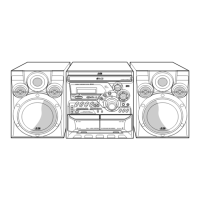
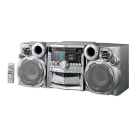
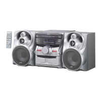
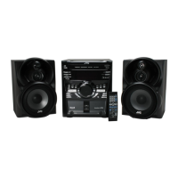
MX-K35V
1-32
TC9462F (IC602) : Digital servo single chip processor
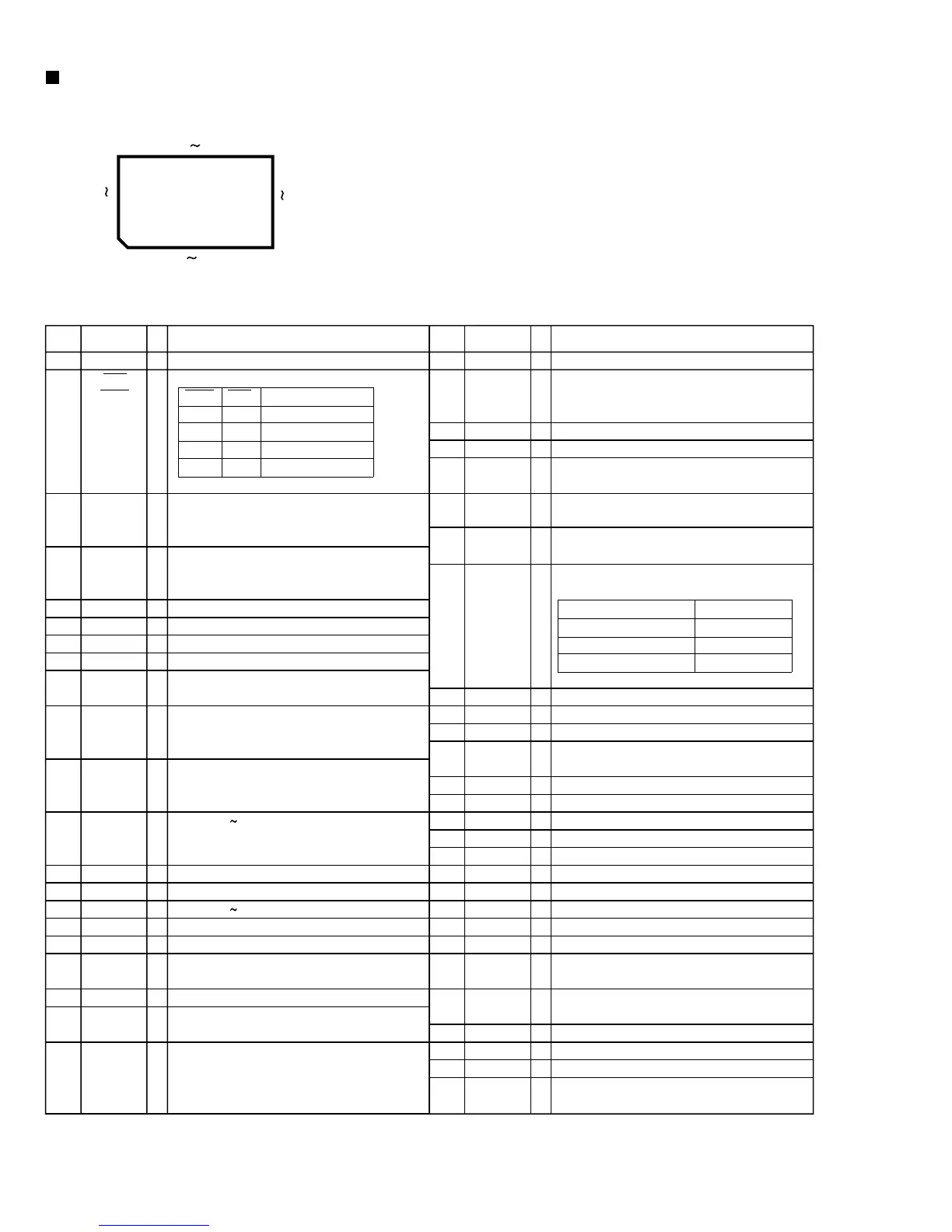
1. Terminal layout
2. Pin function
Symbol I/OPin No. Symbol I/O Function
1
2
3
4
5
6
7
8
9
10
11
12
13
14
15
16
17
18
19
20
21
22
TEST0
HSO
UHSO
EMPH
LRCK
VSS
BCK
AOUT
DOUT
MBOV
IPF
SBOK
CLCK
VDD
VSS
DATA
SFSY
SBSY
SPCK
SPDA
COFS
MONIT
Test mode terminal. Normally, keep at open
Playback speed mode flag output terminal.
UHSO HSO PLAYBACK SPEED
H H Normal
H L 2 times
L H 4 times
L L -
Subcode Q data emphasis flag output terminal.
Emphasis ON at "H" level and OFF at "L" level.
The output polarity can invert by command.
Channel clock output terminal. (44.1kHz)
L-ch at "L" level and R-ch at "H" level. The
output polarity can invert by command.
Digital ground terminal.
Bit clock output terminal. (1.4112MHz)
Audio data output terminal.
Digital data output terminal.
Buffer memory over signal output terminal.
Over at "H" level.
Correction flag output terminal.
At "H" level, AOUT output is made to correction
impossibility by C
2 correction processing.
Subcode Q data CRCC check adjusting result
output terminal. The adjusting result is OK at
"H" level.
Subcode P
W data readout clock input/output
terminal. This terminal can select by command
bit.
Digital power supply voltage terminal.
Digital ground terminal.
Subcode P
W data output terminal.
Playback frame sync signal output terminal.
Subcode block sync signal output terminal.
Processor status signal readout clock output
terminal.
Processor status signal output terminal.
Correction frame clock output terminal.
(7.35kHz)
Internal signal (DSP internal flag and PLL
clock) output terminal. Selected by command.
This terminal output the text data with serial
by command.
I
O
O
O
O
-
O
O
O
O
O
O
I/O
-
-
O
O
O
O
O
O
O
80 51
1
30
100 81
31
50
23
24
25
26
27
28
29
30
31
32
33
34
35
36
37
38
39
40
41
42
43
44
45
46
47
48
49
50
VDD
TESIO0
P2VREF
HSSW
ZDET
PDO
TMAXS
TMAX
LPFN
LPFO
PVREF
VCOREF
VCOF
AVSS
SLCO
RFI
AVDD
REFCT
RFZI
RFRP
FEI
SBAD
TSIN
TEI
TEZI
FDO
TRO
VREF
Digital power supply voltage terminal.
Test input/output terminal. Normally, keep at
"L" level. The terminal that inputted the clock
for read of text data by command.
PLL double reference voltage supply terminal.
2/4 times speed at "V
REF" voltage.
1 bit DA converter zero detect flag output
terminal.
Phase difference signal output terminal of
EFM signal and PLCK signal.
TMAX detection result output terminal.
Selected by command bit (TMPS).
TMAX detection result output terminal.
Selected by command bit (TMPS).
DIFFERENCE RESULT TMAX OUTPUT
Longer than fixed freq. "P2V
REF"
Shorter than fixed freq. "Vss"
Within the fixed freq. "HiZ"
LPF amplifier inverting input terminal for PLL.
LPF amplifier output terminal for PLL.
PLL reference voltage supply terminal.
VCO center frequency reference level terminal.
Normally, keep at "PV
REF" level.
VCO filter terminal.
Analog ground terminal.
Data slice level output terminal.
RF signal input terminal.
Analog power supply voltage terminal.
RFRP signal center level input terminal.
RFRP zero cross input terminal.
RF ripple signal input terminal.
Focus error signal input terminal.
Sub-beam adder signal input terminal.
Test input terminal. Normally, keep at "V
REF"
level.
Tracking error signal input terminal.
Take in at tracking servo on.
Tracking error zero cross input terminal.
Focus servo equalizer output terminal.
Tracking servo equalizer output terminal.
Analog reference voltage supply terminal.
-
I
-
O
O
O
O
O
I
O
-
I
O
-
O
I
-
I
I
I
I
I
I
I
I
O
O
-
Pin No. Function
 Loading...