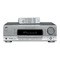
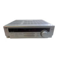
RX-5030VBK
(No.22025)1-13
Note:
(1) SDOS, SMUTE, DFS, and LOOP1 pins are ORed with register data if P/S = "L".
(2) The group 1 and 2 can be selected by DZFM2-0 bit if P/S = "L" and DZFME = "L".
(3) This pin becomes OVF pin if OVFE bit is set to "1" at serial control mode.
(4) All input pins should not be left floating.
19 ICKS - Connect to GND No internal bonding.
20 ADIF - Analog Input Format Select Pin, Digital Power Supply
H : Full-differential input "L" : Single-ended input
21 CAD1 - Chip Address 1 Pin, Connect to GND
22 CAD0 O Chip Address 0 Pin, Connect to GND
23 LOUT3 O DAC3 Lch Analog Output Pin
24 ROUT3 O DAC3 Rch Analog Output Pin
25 LOUT2 O DAC2 Lch Analog Output Pin
26 ROUT2 O DAC2 Rch Analog Output Pin
27 LOUT1 O DAC1 Lch Analog Output Pin
28 ROUT1 O DAC1 Rch Analog Output Pin
29 LIN- I Lch Analog Negative Input Pin
30 LIN+ I Lch Analog Positive Input Pin
31 RIN- I Rch Analog Negative Input Pin
32 RIN+ I Rch Analog Positive Input Pin
33 VREFL - Zero Input Detect 2 Pin (Note 2), Non Connect
When the input data of the group 1 follow total 8192LRCK cycles with "0" input data,
this pin goes to "H".
OVF O Analog Input Overflow Detect Pin (Note 3)
This pin goes to "H" if the analog input of Lch or Rch is overflows.
34 VCOM O Common Voltage Output Pin, AVDD/2
Large external capacitor around 2.2uF is used to reduce power-supply noise.
35 VREFH - Positive Voltage Reference Input Pin, AVDD
36 AVDD - Analog Power Supply Pin, 4.5V~5.5V
37 AVSS - Analog Ground Pin, 0V
38 XTI - Zero Input Detect 1 Pin (Note 2) Non connect
When the input data of the group 1 follow total 8192 LRCK cycles with "0" input data,
this pin goes to "H".
39 XTO I Master Clock Input Pin
40 P1S - Parallel / Serial Select Pin
"L" : Serial control mode, "H" : Parallel control mode
41 CS
I Audio Data Interface Format 0 Pin in parallel mode
CSN I Chip select pin in 3-wire serial control mode
This pin should be connected to DVDD at I2C bus control mode
42 DIF1 I Audio Data Interface Format 1 Pin in parallel mode
SCL/CCLK I Control Data Clock Pin in serial control mode
I2C = "L" : CCLK(3-wire Serial), I2C = "H" : SCL(I2CBus)
43 LOOP0 I Loopback Mode 0 Pin in parallel control mode
Enables digital loop-back from ADC to 3 DACs.
SAD/CDTI I/O Control Data Input Pin in serial control mode
I2C = "L" : CDTI(3-wire Serial), I2C = "H" : SDA(I2CBus)
44 CDTD I Loopback Mode 1 Pin (Note 1)
Enable all 3 DAC channels to be input from SDTII.
No. Symbol I/O Function
 Loading...