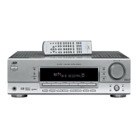
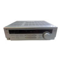
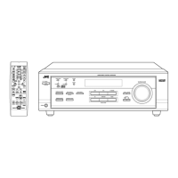
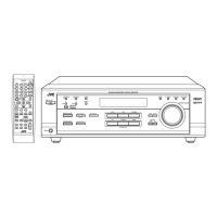
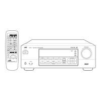
RX-5030VBK
1-26 (No.22025)
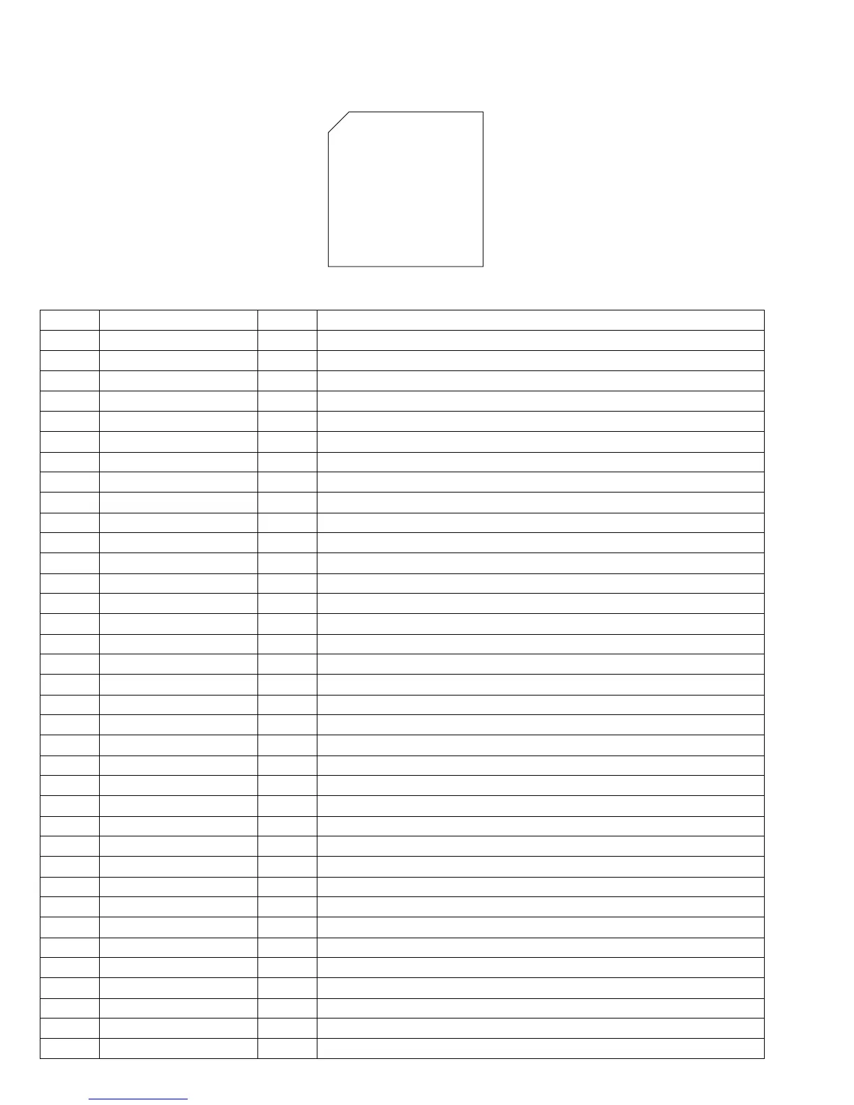
4.20 UPD784215AGC167 (IC671): Digital signal controller
• Pin layout
• Pin function
1
25
75
51
100 76
26 50
~
~
~
~
Pin No. Symbol I/O Function
1~8 - Non connect
9 VDD - Power supply terminal
10 X2 O Connecting the crystal oscillator for system main clock
11 X1 I Connecting the crystal oscillator for system main clock
12 VSS - Connect to GND
13 XT2 O Connecting the crystal oscillator for system sub clock
14 XT1 I Connecting the crystal oscillator for system sub clock
15 RESET I System reset signal input
16 AUTODATA I Output of DSP to general-purpose port
17 LOCK I Output of DSP to general-purpose port
18 DIGITAL0 I Output of DSP to general-purpose port
19 FORMAT I Output of DSP to general-purpose port
20 CHANNEL I Output of DSP to general-purpose port
21 ERR I Output of DSP to general-purpose port
22 REST IN I Reset signal input
23 AVDD - Power supply terminal
24 AVREF0 - Connect to GND
25 - Connect to GND
26 - Connect to GND
27 - Connect to GND
28 - Connect to GND
29 - Connect to GND
30 - Connect to GND
31 - Connect to GND
32 - Connect to GND
33 AVSS - Connect to GND
34,35 - Non connect
36 AV REF1 - Power supply terminal
37 RX - Not use
38 TX - Not use
39 - Non connect
40 DSPCOM I Communication port from IC701
41 DSPSTS O Status communication port to IC701
42 DSPCLK I Clock input from IC701
43 DSPRDY I Ready signal input from IC701
44 - Non connect
 Loading...