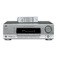
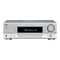
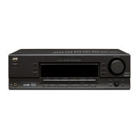
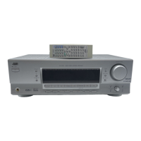
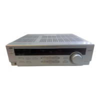
RX-5030VBK
(No.22025)1-25
4.19 TC9446F-025 (IC631): Digital signal processor for dolby digital (AC-3) / DTS audio decode
• Pin Function
Pin No. Symbol I/O Function
1 RST I Reset signal input terminal (L:reset H: normal operation)
2 MIMD I Microcomputer interface mode selection input terminal (L:serial H:IC bus)
3 MICS I Microcomputer interface chip select input terminal
4 MILP I Microcomputer interface latch pulse input
5 MIDIO I/O Microcomputer interface data I/O terminal
6 MICK I Microcomputer interface clock input terminal
7 MIACK O Microcomputer interface acknowledge output terminal
8~11 FI0~3 I Flag input terminal 0~3
12 IRQ I Interrupt input terminal
13 VSS - Digital ground terminal
14 LRCKA I Audio interface LR clock input terminal A
15 BCKA I Audio interface bit clock input terminal A
16~18 SDO0~2 O Audio interface data output terminal 0
19 SD03 - Non connect
20 LRCKB I Audio interface LR clock input terminal B
21 BCKB I Audio interface bit clock input terminal B
22 SDT0 I Audio interface data input terminal 0
23 SDT1 I Audio interface data input terminal 1
24 VDD - Power supply for digital circuit
25 LRCKOA O Audio interface LR clock output terminal A
26 BCKOA O Audio interface bit clock output terminal A
27, 28 TEST0,1 I Test input terminal 0/1 (L:test H: normal operation)
29~30 LRCKOBBCKOB - Non connect
31 TXO O SPDIF Output
32, 33 TEST2,3 I Test input terminal (L:test H: normal operation)
34 RX I SPDIF input terminal
35 VSS - Ground terminal for digital circuit
36 TSTSUB0 I Test sub input terminal 0 (L:test H: normal operation)
37 FCONT O VCO Frequency control output terminal
38, 39 TSTSUB1TSTSUB2 I Test sub input terminal 12 (L:test H: normal operation)
40 PDO O Phase detect signal output terminal
41 VDDA - Power supply for analog circuit
42 PLON I Clock selection input terminal (L:external clock H:VCO clock)
43 AMPI I amplifier input terminal for LPF
44 AMPO O amplifier output terminal for LPF
45 CKI I External clock input terminal
46 VSSA - Ground terminal for analog circuit
47 CKO O DIR Clock output terminal
48 LOCK O VCO Lock output terminal
49 VSS - Ground terminal for digital circuit
50 WR O External SRAM writing signal output terminal
51 OE O External SRAM output enable signal output terminal
52 CE O External SRAM chip enable signal output terminal
53 VDD - Power supply terminal for digital circuit
54~61 IO7~0 I/O External SRAM data I/O terminal 7~0
62 VSS - Ground terminal for digital circuit
63~70 AD0~7 O External SRAM address output terminal 0~7
71 VDD - Power supply terminal for digital circuit
72~80 AD8~16 O External SRAM address output terminal 8~16
81 VSS - round terminal for digital circuit
82~89 PO0~7 O General purpose output terminal 0~7
90 VDDDL - Power supply terminal for DLL
91 LPFO O LPF output terminal for DLL
92, 93 DLON,DLCKS I Refer to the undermentioned table
94 SCKO - Non connect
95 VSSDL - Ground terminal for DLL
96 SCKI I External system clock input terminal
97 VSSX - Ground terminal for oscillation circuit
98, 99 XO,XI I/O Oscillation I/O terminal
100 VDDX - Power supply terminal for oscillation circuit
DLCKS terminal DLON terminal DLL clock setting
L L SCKI input (DLL circuit OFF)
L H Four times XI clock
H L Three times XI clock
H H Six times XI clock
 Loading...