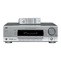
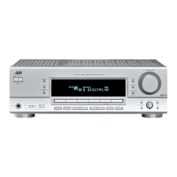
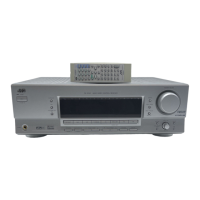
RX-5030VBK
1-12 (No.22025)
SECTION 4
Description of major ICs
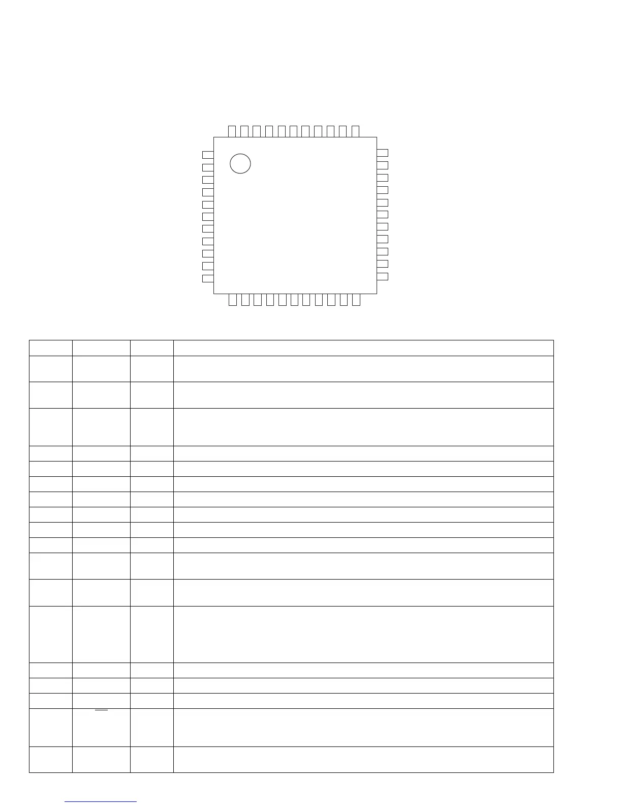
4.1 AK4527BVQP (IC601): A/D, D/A converter
• Pin layout
• Pin function
1
2
3
4
5
6
7
8
9
10
11
33
32
31
30
29
28
27
26
25
24
23
12
13
14
15
16
17
18
19
20
21
22
44
43
42
41
40
39
38
37
36
35
34
Top View
No. Symbol I/O Function
1 SDOS I SDTO Source Select Pin (Note 1)
"L" : Internal ADC output, "H" : DAUX input
2 OSKS I Control Mode Select Pin
"L" : 3-wire Serial, "H" : I2C Bus
3 MIS - Soft Mute Pin (Note 1) Connect to GND
When this pin goes to "H" soft mute cycle is initialized.
When returning to "L", the output mute releases.
4 BICK I Audio Serial Data Clock Pin
5 LRCK I/O Input Channel Clock Pin
6 SDTI1 I DAC1 Audio Serial Data Input Pin
7 SDTI2 I DAC2 Audio Serial Data Input Pin
8 SDTI3 I DAC3 Audio Serial Data Input Pin
9 SDTO O Audio Serial Data Output Pin
10 D,AUX - Sub Audio Serial Data Input Pin, Connect to GND
11 DFS - Double Speed Sampling Mode Pin (Note 1)
"L" : Normal Speed, "H" : Double Speed
12 DEMI - Connect to GND
No internal bonding.
13 DEMO - Zero Input Detect Enable Pin, Connect to GND
"L" : mode 7 (disable) at parallel mode,
- zero detect mode is selectable by DZFM2-0 bits at serial mode.
- H : mode 0 (DZF is AND of all six channels)
14 MCKO - Output Buffer Power supply Pin, 2.7V~5.5V
15 DVDD I Digital Power Supply Pin, 4.5V~5.5V
16 DVSS - De-emphasis Pin, 0V
17 PD
I Power-Down & Reset Pin
When "L", the AK4527B is powered-down and the control registers are reset to default state.
If the state of P/S or CAD0-1 changes, then the AK4527B must be reset by PDN.
18 XTS - Test Pin, Connect to GND
This pin should be connected to DVSS.
 Loading...