XV-SA600BK/XV-SA602SL
31
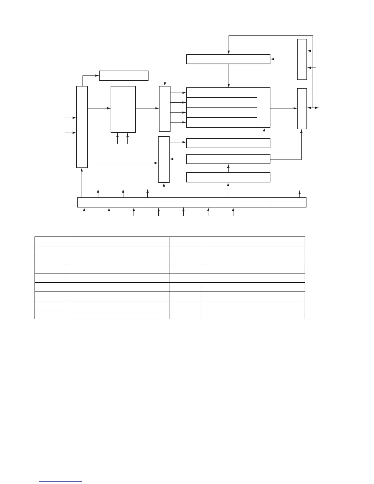
4.5 K4S643232E-TC60(IC505):DRAM
4.5.1 Block diagram
4.5.2 Pin function
Bank select
Address register
Row buffer
refresh counter
LRAS
LRAS
LCBR
LCBR LWE
LK
DD
LCKE
Row decoder
Col. buffer
LCAS LWCBR
CLK CKE CS RAS CAS WE DQM
LDQM
Timing register
Data input register
512K x 32
512K x 32
512K x 32
512K x 32
I/O control
Sense AMP
Output buffer
LWE
LDQ
DQ
Column decoder
Latency & burst length
Programming register
Symbol Description Symbol Description
CLK System clock signal input DQM0~3 Data input/output mask
CS Chip select input DQ0~31 Data input/output
CKE Clock enable VDD Power supply terminal
A0~A10 Address VSS Connect to ground
BA0,1 Bank select address VDDQ Power supply terminal
RAS Row address strobe VSSQ Connect to ground
CAS Column address strobe NC Non connect
WE Write enable
 Loading...