PT8100 Service Manual
5
CF1 is cut off; when the mobile radio is set to narrowband, CF1
is put through and takes effect, while CF2 is cut off.
Squelch circuit
The demodulated signal from IC6 is sent to the internal noise
amplifier in IC6. Then the resulting signal is further amplified in
Q21 and demodulated in D25, and then the resulting DC level is
sent to the MCU squelch control circuit. This voltage is in inverse
proportion to the input signal.
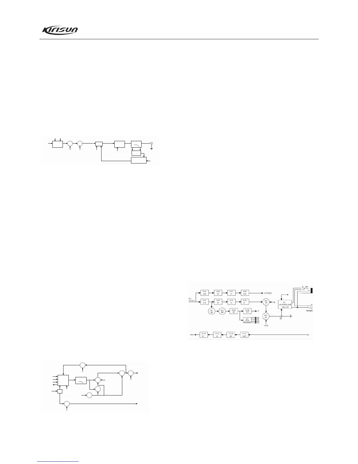
4.3 Principle of Transmitter (TX)
TX power amplification
VCO
RF AMP
8T 8R
Q4
Q5
DRIVE
PRE
8T
8T
ANT S W
LPF
APC CONTROL
IC4
TX/ RX SW
TO ANT
IC1
RA30H
APC
8T
13.8V
Figure 4.3 Principle of Power Amplifier and Antenna Switch
The modulated RF signal from VCO is amplified by Q1, Q2,
Q4, and Q5, and is sent to IC1 for power amplification. Output
power of IC1: 25W.
Grid bias of IC1 is controlled by the APC circuit. Through
changing the grid bias voltage, the Tx output power can be
controlled conveniently.
APC(Automatic Power Control)circuit
D9 and D10 are RF detector diodes. The output power of the
RF amplifier is detected by RF detector diodes and converted into
DC level. Then the DC level is compared with the signal from
MCU and amplified in IC4, and is sent to grid in IC1 to control
the power output.
If the Tx output power is too high, the voltage detected by the
detector diodes will increase; IC4 output voltage will decrease, so
the bias voltage imposed on IC1 will also decrease, which causes
the Tx output power to be lowered, and vice versa. Thus, the Tx
output power can keep stable under different working conditions.
MCU can set the power through changing the voltage input to
IC4.
4.4 Principle of Frequency Synthesizer
UL
CK
DT
UL
PLL IC
IC3
QT TCXO
5V
LOOP FILTER
RIPPLE
FILTER
VCO
Q6
BUFF
Q1 Q2
RF AMP
VCO OUT
5V
Q14
2ND LOCAL
MB15E03SL
MOD
16.8MHz
X1
TCXO
3.5V
TX
VCO
Q14
RX
8R
Q11
*3 2ND LOCAL AMP
Q7
BUFF
5V
Figure 4.4 Frequency Synthesizer
PT8100 adopts PLL type frequency synthesizer.
The frequency synthesizer consists of reference oscillator,
voltage control oscillator (VCO), programmable divider, phase
comparator, and low pass filter (LPF).
Tx VCO unit consists of Q6, D1, D4, D5, and D6. D8 is the
modulation circuit of Tx VCO.
Rx VCO unit consists of Q12, D14, D16, D17 and D18.
IC3 (MB15E03SL) is the PLL integrated circuit, which
consists of programmable reference divider, programmable
divider, phase comparator, and charge pump.
The low pass filter consists of R54 and C113.
The reference frequency is provided by X1 (TCXO,
16.8MHz).
Reference frequency from TCXO (Temperature-Controlled
Crystal Oscillator) is divided by the programmable reference
divider in IC3 to produce reference frequency of 5kHz or
6.25kHz (determined by the preset channel frequency and is
controlled by MCU).
The oscillation frequency from VCO goes to IC3 where it is
divided by the programmable divider and is then compared with
the reference frequency to obtain the error signal. The signal is
then filtered by a low pass filter and is sent to VCO to change the
oscillation frequency of the VCO, enabling the frequency to
reach the set value. Then the VCO is locked.
Unlock detection: When PLL is unlocked, pin14 of IC3 will
output low level signal to MCU. Then MCU prohibits the Tx
from transmitting and makes an alert tone.
4.5 Audio Processing Circuit
Figure 4.5 Audio Processing
MIC signal processing:
Voice signal from MIC is sent to IC13A for amplification
(IC13A, D32, Q32 and other components form the AGC circuit to
improve the dynamic range of the circuit). Then the resulting
signal is pre-emphasized by C322 and R267 and goes to the IDC
circuit consists of IC13B. After being limited, the signal is
switched into wideband or narrowband in Q30 and then passes
through the low pass circuit consists of IC13C and IC13D to
remove signals above 3000Hz. Then the filtered signal is sent to
VR2 to adjust the deviation and modulated by D8, and then is