
B
brent79Aug 2, 2025
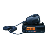
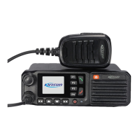
What to do if Kirisun PT8100 -01 Radio has abnormal programming?
- MmatthewcooperAug 2, 2025
If you are experiencing abnormal programming with your Kirisun Radio, consider the following: * Check the programming cable connection to ensure it is properly connected. * Verify the RS-232 serial port output of your computer. * Inspect the radio’s socket for the programming cable for any contact issues. If the socket is faulty, replace it.