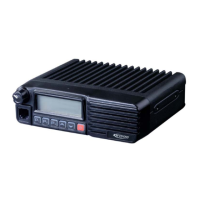
PT8100 Service Manual
7
4 74.4 14 103.5 24 146.2 34 210.7
5 77.0 15 107.2 25 151.4 35 218.1
6 79.7 16 110.9 26 156.7 36 225.7
7 82.5 17 114.8 27 162.2 37 233.6
8 85.4 18 118.8 28 167.9 38 241.8
9 88.5 19 123.0 29 173.8 39 250.3
10 91.5 20 127.3 30 179.9
DCS
DCS (Digital Code Squelch), which is used to control squelch,
is a series of continuous digital codes modulated on carrier
together with voice signal. If DCS is set, the speaker can be
opened only when the radio receives signal with the same DCS to
avoid disturbance of unwanted signals.
PT8100 has 83 standard codes (inverted and non-inverted) for
your selection. See Table 4.2.
DCS signal (PWM wave) is produced by MCU. It passes
through the low pass filter consists of RC to remove the high
frequency components (above 300Hz). Then the resulting signal
is sent to VCO and TCXO for modulation, with HF components
of the DCS signal being modulated by VCO, and the LF
components of the DCS signal being modulated by TCXO.
The DCS signal coming from the receiver is routed to MCU
for decoding. MCU checks if the DCS code in the received signal
matches the preset DCS of the radio, and determines whether to
open the speaker or not.
Table 4.2 DCS Codes
023 114 174 315 445 631
025 115 205 331 464 632
026 116 223 343 465 654
031 125 226 346 466 662
032 131 243 351 503 664
043 132 244 364 506 703
047 134 245 365 516 712
051 143 251 371 532 723
054 152 261 411 546 731
065 155 263 412 565 732
071 156 265 413 606 734
072 162 271 423 612 743
073 165 306 431 624 754
074 172 311 432 627
4.9 Semiconductor Data
MCU Description
Table 4.3 Port Description of MCU (MB90F882)
No. Port name
Pin
Name
I/O Function
1 GLED P40 O Rx Green Indicator H: on
2NC
3 NC - -
4 NC - -
5 P5 P32 I P5 Button Input
6 P1 P33 I P1 Button Input
7 P2 P34 I P2 Button Input
8 P3 P35 I P3 Button Input
9 P4 P36 I P4 Button Input
10 POWER P37 I Power Button Input
11 NC
12 NC
11 NC - -
12 NC - -
13 VCC VCC - CPU Power Input
14 VSS VSS - GND
15 C C -
16 LCD RST P42 O LCD Reset Control
17 LCD BLC P43 O LCD Backlight Control
18 LCD DAT P44 I/O LCD Serial Data Input/Output
19 LCD WR P45 O LCD Write Clock Output
20 LCD RD P46 O LCD Read Clock Output
21 LCD CS P47 O LCD Chip Selection Signal Output
22 MICDAT P90 I
Reserved: Hand MIC Digital Keypad Data
Input
23 HOOK P91 I Hook Signal Input
24 DEV2 P92 O Max. Deviation Compensation
25 DEV1 P93 O
26 UL P94 I
PLL Unlock Detect Pin
H:Locked,L:Unlocked
27 CK P95 O PLL Clock Output
28 LE P96 O PLL IC Enable Pin
29 DT P97 O PLL Data Output
30 AVCC AVCC - Connect with VCC
31 AVRH AVRH - Connect with VCC
32 NC - -
33 AVSS AVSS - Connect with VSS
34 QT/DQT IN AN0 I(A/D0) QT/DQT Signal Input
35 RSSI AN1 I(A/D1) Signal Strength Input
36 BUSY AN2 I(A/D2) Busy Signal Input
37 TEMP AN3 I(A/D3) Power Amplifier Temperature Protection Input
38 NC - -
39 NC - -
40 NC - -
41 NC - -
42 VSS VSS - GND
43 DTMFD0 P71 I DTMF Detect Input
44 DTMFD1 P72 I DTMF Detect Input
45 DTMFD2 P73 I DTMF Detect Input
46 DTMFD3 P74 I DTMF Detect Input
47 RX P76 O
TX/RX VCO Selection
H: TX, L: RX
48 DTMFDV P75 I DTMF Decoding Valid Input
49 MD2 MD2 - Programming Test Point
50 MD1 MD1 - Programming Test Point
51 MD0 MD0 - Programming Test Point
52 RESET RST I Programming Test Point
53 SCL UI6 O E
2
PROM Clock Line
54 SDA UO6 I/O
55 TEST P82 O L:Writable
56 NC
57 RXD P84 I RS-232 Input, Programming Test Point
58 TXD P85 O RS-232 Output, Programming Test Point
59 NC - -
60 NC - -
61 NC - -