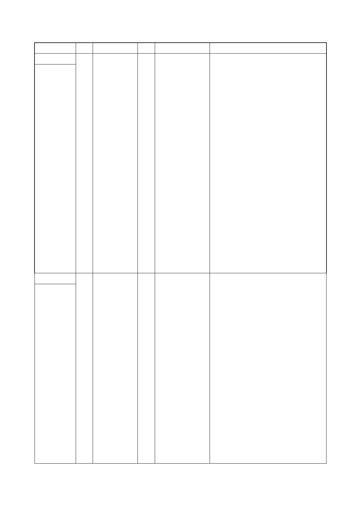
2T6/2T7/2T8/2T9
2-3-10
YC19 1 ENVSENSN I 0/3.3 V DC ENVS: On/Off
Connected to
the high volt-
age PWB
2 GND - - Ground
3 MISENS I Analog MC output signal
4 MHVCLK O 0/3.3 V DC (pulse) MC clock signal
5 MACCNT O Analog MC AC control signal
6 MDCCNT O Analog MC DC control signal
7 HVCLK O 0/3.3 V DC (pulse) DEV clock signal
8 BDCNT O Analog DEV DC control signal
9 BACNT O Analog DEV AC control signal
10 PAPERSEN2
N
I 0/3.3 V DC EFS2: On/Off
11 PAPERSEN1
N
I 0/3.3 V DC EFS1: On/Off
12 REGSENSN I 0/3.3 V DC RS: On/Off
13 DUJAMSEN2
N
I 0/3.3 V DC DUS: On/Off
14 +3.3V3_F2 O 3.3 V DC 3.3 V DC power output to HVPWB
15 SCNT O 0/3.3 V DC Separation output control signal
16 TRREM O 0/3.3 V DC TC remote signal
17 TCNT O Analog TC control signal
18 +24V3_IL O 24 V DC 24 V DC power output to HVPWB
YC20 1 +24V0 O DC24V 24 V DC power output
Connected to
the main
PWB
2 +24V0 O DC24V 24 V DC power output
3 +24V0 O DC24V 24 V DC power output
4 +3.3V0_PM I DC3.3V 3.3 V DC power input
5 +3.3V3_E I DC3.3V 3.3 V DC power input
6 +3.3V3_E I DC3.3V 3.3 V DC power input
7 +5.0V1_C1 I DC5.0V 5 V DC power input
8 +3.3V1_C I DC3.3V 3.3 V DC power input
9 DUTY_CONT
ROL
I DC0V/3.3V(pulse)
10 E2C_SDAT O DC0V/3.3V Serial communication data input
11 C2E_SDAT I DC0V/3.3V Serial communication data output
12 C2E_SCK I DC0V/3.3V Serial communication clock signal
13 E2C_SDIR O DC0V/3.3V Serial communication direction signal
14 E2C_SBSY O DC0V/3.3V System busy signal
15 GND - - Ground
16 VBUS_USBH
_3
I DC0V/5.0V 5 V DC power input to USB
Connector Pin Signal I/O Voltage Description
 Loading...