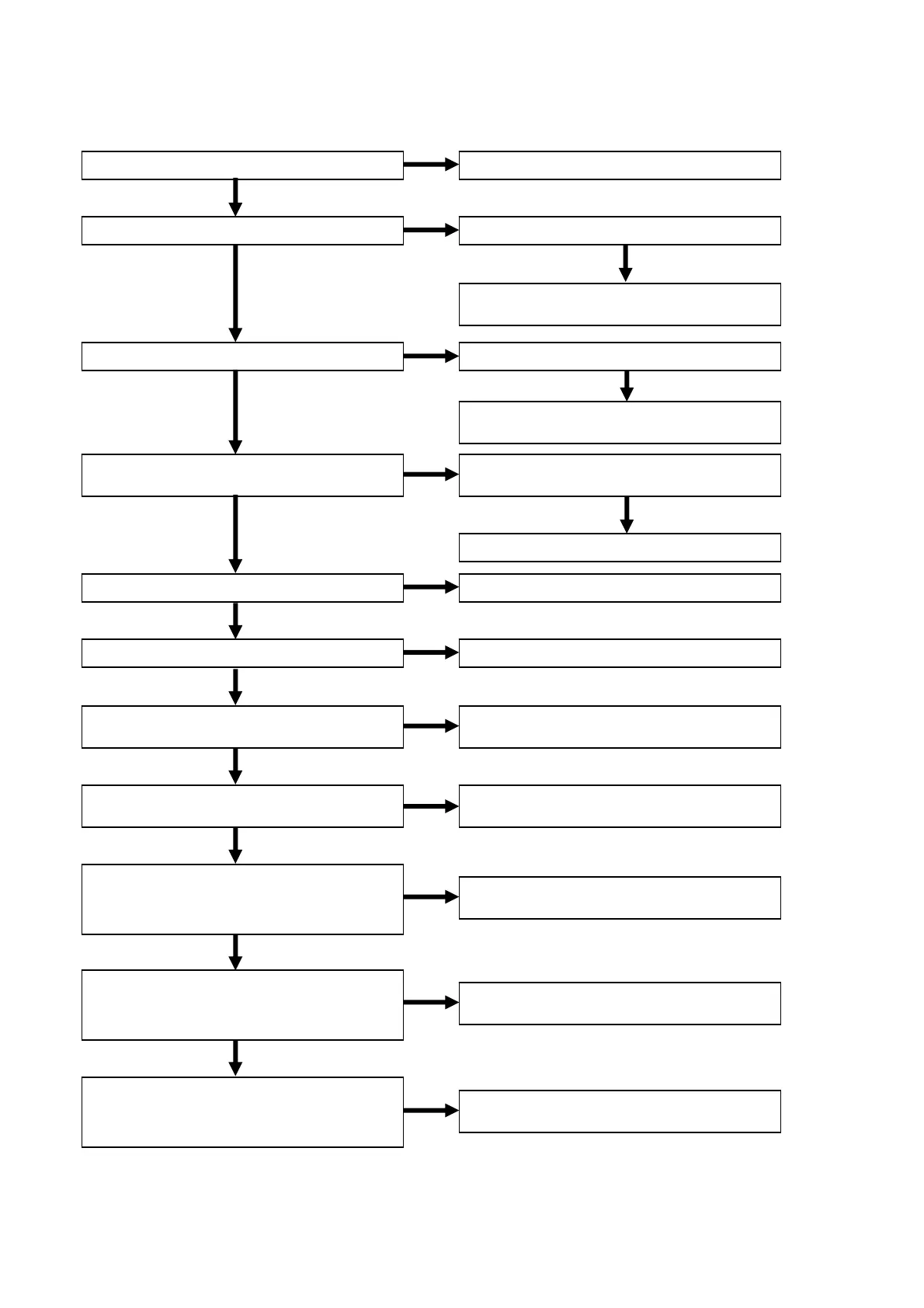
64
7. IEEE1394 PWB (PI01)
7.1 Check the i.Link.
Is the E+6V voltage line (JI61) normal? Refer to “1. POWER SUPPL
PWB (P801)”.
Is the 14pin of JI62 H?
Refer to “3.1 Check the panel
microprocessor”.
OK
Is the +3.3VU line (QJ01) normal?
Check the soldering of JI62.
NG
NG
Is the 1 pin of JI62 H?
Check the soldering of QI90 and the
input/output voltage.
OK
NG
Check the soldering of FJ01.
OK
OK
Check the soldering of FI01.
NG
Refer to “3.1 Check the panel
microprocessor”.
Check the soldering of JI62.
OK
Is the +3.3VD line (QI01) normal?
Check the soldering of FI02.
OK
Check the soldering of XJ01,
circumference components and QJ01.
Check the soldering of XI01,
circumference components and QI01.
Check the soldering of JI62,
circumference components and QI01.
Check the soldering of JI60,
circumference components and QI01.
Check the soldering of JI60 and JI62
circumference components and QI01.
NG
Is the +3.3VA line (QJ01) normal?
Are the clock wave form of 89pin on
QJ01 normal? (16MHz, 3Vp-p)
Are the clock wave form of 53pin on QI01
normal? (24.576MHz, 3Vp-p)
Play DVD-Audio Disc.
Are the signal wave form of 9 to 18pin on
QI01 normal?
NG
NG
NG
NG
NG
NG
OK
Play SACD Disc. Are the signal wave
form of 158,159 and 163 to 167pin on
QI01 normal?
Play CD Disc.
Are the signal wave form of 169 and
173pin on QI01 normal?
OK
OK
OK
OK
OK
OK