dsPIC33CH Curiosity Development Board User’s Guide
DS50002762A-page 16
Advance Information
2018 Microchip Technology Inc.
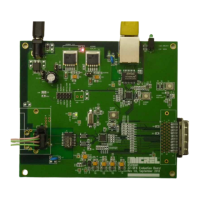
J13 – This jumper sets the effective resistor divider feedback ratio for the SMPS output
voltage when it is measured by the U1 ADC. When the SMPS is used to generate rel-
atively low voltages (ex: 0V-6.5V), it is suggested to keep J13 capped to maximize
feedback circuit sensitivity. When the SMPS will be used to generate voltages above
6.5V, J13 should be opened to ensure the feedback voltage stays within the input
sensing range of the ADC.
J14 – This is an unpopulated 2-pin jumper location that can be used to disconnect the
SMPS transient generator circuitry from the output of the SMPS circuit. In order to
disconnect the transient generator circuit, it is suggested to populate J14 with a 2-pin
jumper header and to cut the trace (NT5) on the bottom of the PCB linking the pins
of J14.
J15 – This is an unpopulated 6-pin staggered header interface that can optionally be
used to connect an external programmer/debugger tool to the target microcontroller U1
when performing dual simultaneous debug of both the Master and Slave cores. The
J15 header connects to the Slave debug port, S1PGx3, and is only intended for use
during dual debug operations. For single core debug of either the Master or Slave,
either J2 or the PKOB circuit should be used. The holes for J15 are slightly staggered,
which provides some friction retention force, without requiring physical soldering, when
a straight male-male or right angle male-male header is installed in J15.
J16 – This is a standard female USB micro-B connector, which connects to the
MCP2221A USB-UART converter chip. This USB interface is a data interface only, as
it is galvanically isolated from the rest of the application circuitry and does not supply
power to the rest of the board.
J17 – This is an unpopulated footprint that may optionally be used to install a standard
DC barrel jack for externally powering the board from a regulated 5.0V wall cube.
J18 – This is a female I/O pin access header for accessing certain U1 microcontroller
I/O pins, along with the various power rails implemented on the development board.
J19 – This is an unpopulated 2-pin jumper header, that may optionally be used as an
attachment point for connecting an external frequency response analyzer tool, for
measuring the SMPS control loop phase/gain characteristics. The 20 Ohm load resistor
(R96) is connected directly across the J19 pins.
J20 – This is a standard female USB micro-B connector that is intended to be used to
power the board and provide a USB communication path when using the integrated
programmer/debugger (PKOB) circuit.
J21 – This is a 2-pin screw terminal that provides access to the SMPS V
OUT
and GND
nets. This is a convenient place for attaching external loads that may be powered by
the SMPS circuit.
2.5.2 SMPS Hardware Overcurrent Protection
The components, Q11, C22, R67, U10, and the high-side current sense resistors,
R59 + R74, implement a crude form of hardware-based overcurrent protection. In a
normal/real application SMPS design, overcurrent protection is often provided through
the use of comparator(s), which would typically be implemented using the comparators
and DACs inside the microcontroller. However, during initial firmware development, the
code for enabling the DACs + comparators may not have been written and debugged
yet, at the time of, say, accidentally dropping an oscilloscope ground lead onto the
demo board. This could result in an unanticipated random short circuit. In these
scenarios, the hardware overcurrent protection circuit implemented by Q11, U10 and
surrounding components can potentially help protect the circuit from damage.