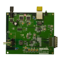
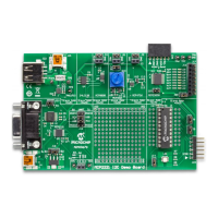
Hardware
2018 Microchip Technology Inc.
Advance Information
DS50002762A-page 19
In the event of improper firmware control of the RC13_TRANSIENT net (e.g., DC logic
high or high time pulses > 10 ms), Q8 would potentially experience high sustained
power dissipation, and unless protected somehow, would be vulnerable to thermal
failure. To prevent this scenario, components, Q10, R88, C51, R90 and R91, imple-
ment a crude maximum on-time restricting sub-circuit, which is intended to limit the Q8
on time to roughly 10 ms maximum.
When RC13_TRANSIENT goes high, C51 begins charging through R88 and will
eventually reach approximately 2x the VBE forward voltage necessary to turn on Q10.
At this point, the output voltage of the resistor dividers, R90 and R91, rises high enough
that Q10 begins turning on, sinking current/voltage away from the gate of Q8 and even-
tually turning off the MOSFET Q8. When RC13_TRANSIENT is eventually driven logic
low, C51 discharges through R90 and R91, resetting the circuit automatically.
2.6 LOW-SIDE CURRENT SENSING
During Buck mode operation, it is sometimes desirable to be able to measure the
current during the off time of MOSFET Q6 if implementing some form of “peak valley”
or Average Current mode control algorithm. Low-side current sensing during the
MOSFET off time is possible via the current sense resistors, R63, R92 and R93. How-
ever, the voltage developed across the current sense resistors will be a negative
voltage with respect to ground. The signal is therefore connected to the inverting input
of one of the PGAs in the microcontroller, which can then be used to invert and amplify
the negative voltage into a positive voltage that can be measured by the ADC or used
by a comparator inside the device.
When supplying a negative input voltage to the PGA, it is important to maintain the I/O
pin voltage within the absolute maximum ratings from the device data sheet, which
allows for negative voltages only within V
SS
to (V
SS
– 300 mV) range. Therefore,
Schottky diode D9 and resistor R95 are used to clamp the negative voltages to within
the 0V to -300 mV range. However, it is important to be aware that the inverting inputs
to the PGAs on the device have approximately 10k typical input impedance from the
device data sheet, and therefore, the resistance of R95 will reduce the gain of the
amplifier for a given PGA setting. Such that, in this configuration, the firmware should
not rely on the absolute output voltage of the PGA to reflect the true current through the
sense resistors, unless the overall gain of the complete circuit is directly measured and
factored into the computations in the firmware.