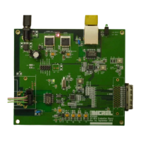
Hardware
2018 Microchip Technology Inc.
Advance Information
DS50002762A-page 17
During an overcurrent condition, when the current through R59 + R74 starts to exceed
approximately 1.2A (ex: 600 mV sense voltage), the base of Q11 will become forward
biased and it will begin to turn on. This will quickly charge the capacitor C22 to the
Schmitt trigger V
IH
input logic high threshold of the U10 logic chip (which is configured
as a Schmitt trigger OR gate). Once the V
IH
level is reached, the U10 output will go high
(independent of the RC14_S1PWM7H signal), thus turning off the high-side P-channel
MOSFET Q6.
At this point, the current through Q6 will drop to zero, Q11 will turn off, but C22 will
remain charged near the V
IH
level until it is eventually bled down to the V
IL
level through
R67. The U10 output will not immediately switch back on due to the Schmitt trigger
hysteresis voltage between the V
IH
and V
IL
input thresholds of U10. It takes approxi-
mately 40% of an RC time constant (between C22 + R67) for the V
IL
threshold to be
reached, which enforces a minimum Q6 off time of roughly 80 µs. This delay is suffi-
cient for the L1 inductor current to drop all the way to zero due to the energy loss in the
diodes D2, D5 and the resistance in the freewheeling current path.
Therefore, even during short-circuit conditions with improperly implemented firmware
control signals, the average current can be maintained at a reasonably safe level. Once
the firmware for enabling and using the internal U1 comparators and DACs has been
developed/debugged, it is expected that the Q11 and related hardware overcurrent
protection components would be omitted, since they would become somewhat
redundant in the final application design.
2.5.3 SMPS Hardware Overvoltage Protection
The components, Q7, C15, R64, R65, R66 and U5, implemented a hardware-based
output overvoltage protection feature in a manner similar to the hardware overcurrent
protection circuit. When a conventional boost converter is operated open loop without
enough load on the output, the output voltage can theoretically rise to an indeterminate
high level, which can potentially avalanche the output Schottky diode, the boost
MOSFET or the output capacitors.
When the output voltage rises above approximately 16V, the output of the resistor
divider (R65 + R66) will become high enough to begin forward biasing the Q7 base and
turning on the transistor. This will quickly discharge C15 from 3.3V down to the V
IL
Schmitt trigger input threshold of the Schmitt AND gate implemented by U5. This over-
rides the PWM control signal and shuts down Q2 until such time as the output
overvoltage condition has decayed away, and enough time has elapsed for R64 to
charge C15 back up to the V
IH
Schmitt trigger input threshold of U5 (automatically
re-enabling PWM activity on Q2).
In a typical/real SMPS application, the closed-loop output feedback control loop would
normally be responsible for preventing output overvoltage conditions from occurring.
However, during initial firmware development, the closed-loop control algorithms may
not yet be fully implemented and operational (or may be halted from normal operation,
for example, due to hitting a debug breakpoint in the firmware). In these scenarios, the
hardware output overvoltage protection circuitry can help to prevent potential circuit
damage.
2.5.4 PWM DAC/DC Bias Generator
The RC5_S1PWM2L net is intended to be driven with a fixed frequency PWM wave-
form. The low-pass filter, consisting of R54 + C26 (and C41 when jumper J10 is
capped), averages the PWM waveforms, and for a high PWM frequency, generates an
adjustable DC voltage. Op amp U8 buffers the DC voltage, providing a low-impedance
firmware adjustable DAC, where the output voltage is based on the PWM duty cycle
provided to the circuit.