PIC® MCU Architecture
2012 Microchip Technology Inc. DS41628B-page 27
Changing pages is necessary in the enhanced core when changing execution from one
page to another. None of the lessons for the enhanced PIC16 occupy more than one
page and, therefore, page changes are not necessary. If the code does overflow into
another page, the assembler will give a warning, indicating that a pagesel may be
required.
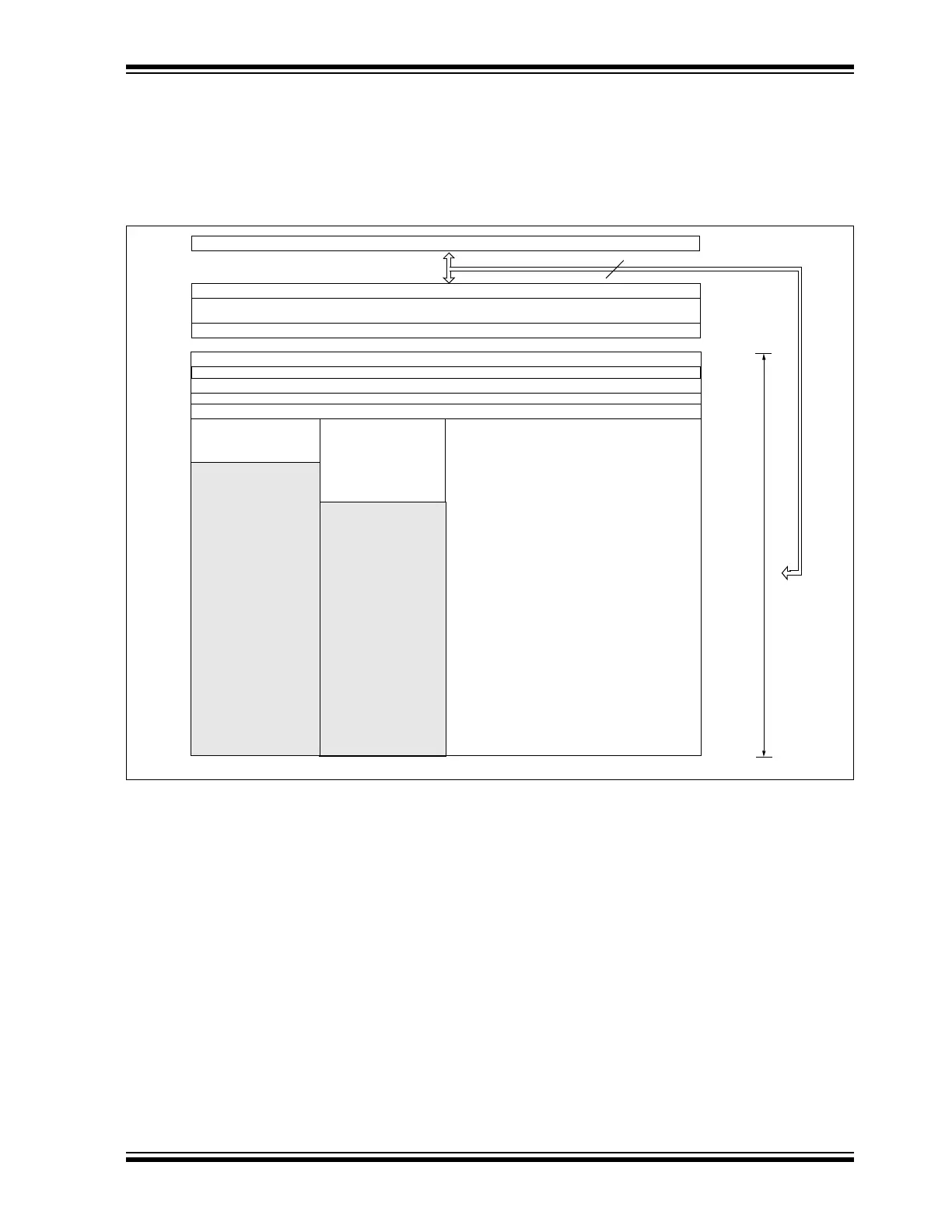
FIGURE 2-7: PIC18 PROGRAM MEMORY MAP AND CALL STACK
2.12.5 User ID
These four memory locations are designated as ID locations where the programmer
can store checksum or other code identification numbers. These are readable and
writable during normal execution.
2.13 DATA MEMORY
The data memory layout of the two device families is perhaps the most significant. Data
memory on both families can be split into four types:
1. Core Registers
2. Special Function Registers
3. General Purpose RAM
4. Common RAM
PC<20:0>
Stack Level 1
Stack Level 31
Reset Vector
Low Priority Interrupt Vector
CALL,RCALL,RETURN
RETFIE,RETLW
21
0000h
0018h
High Priority Interrupt Vector
0008h
User Memory Space
1FFFFFh
4000h
3FFFh
200000h
On-Chip
Program Memory
Read ‘0’
1FFFh
2000h
On-Chip
Program Memory
Read ‘0’
PIC18(L)F14K22
PIC18(L)F13K22