PIC® MCU Architecture
2012 Microchip Technology Inc. DS41628B-page 29
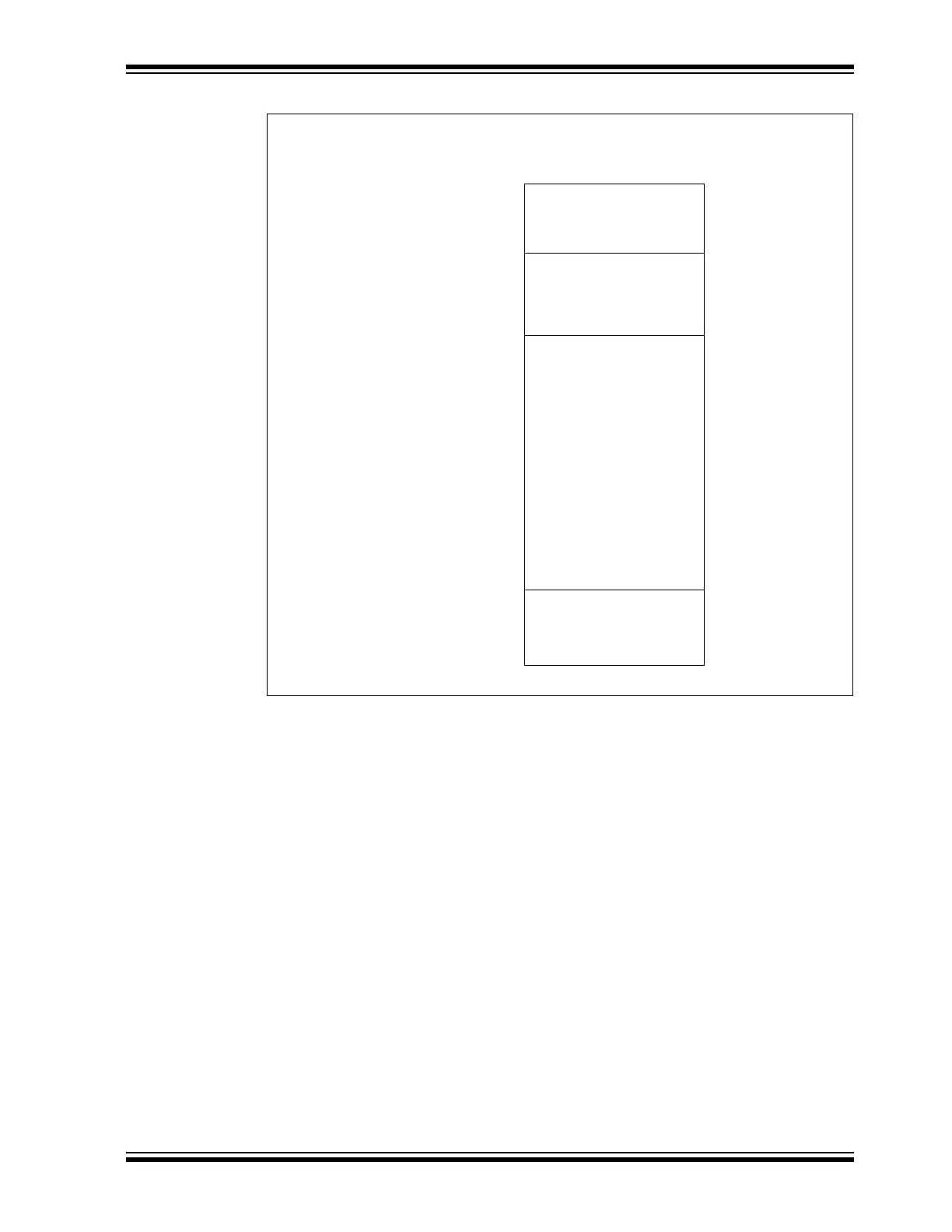
FIGURE 2-8: ENHANCED MID-RANGE BANKED MEMORY PARTITIONING
Addresses 70h-7Fh are shared by all of the banks. This is useful for storing a few bytes
of RAM without the need to switch banks each time the byte is used. Figure 2-9 shows
the first eight banks on the PIC16F1829. Notice how the top 12 core registers are
accessible from every bank, as are the 16 bytes of common RAM.
0Bh
0Ch
1Fh
20h
6Fh
70h
7Fh
00h
Common RAM
(16 bytes)
General Purpose RAM
(80 bytes maximum)
Core Registers
(12 bytes)
Special Function Registers
(20 bytes maximum)
Memory Region
7-bit Bank Offset