EasyManua.ls Logo

miniDSP USBStreamer Box - I2 S;TDM Pinout Diagrams

miniDSP USBStreamer Box
25 pages
Print Icon
To Next Page IconTo Next Page
To Previous Page IconTo Previous Page
Loading...
miniDSP Ltd, Hong Kong / www.minidsp.com / Features and specifications subject to change without prior notice 8
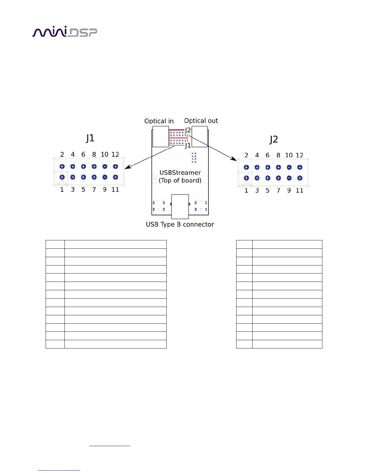
2.2.1 I2S/TDM Pinouts
The USBStreamer circuit board has two 12-pin headers located between the optical ports. All I2S lines are on J1,
while J2 carries auxiliary signaling and GPIO lines reserved for future enhancement. The I2S lines are explained in
detail on the next page.
Note that all I2S lines are 3.3V logic levels. Connected circuits must use a compatible logic level.
Pin
Description
Pin
Description
1
I2S data OUT Ch 1&2 / TDM Out
1
Ground (GND)
2
I2S data IN Ch 1&2 / TDM In
2
NC
3
I2S data OUT Ch 3&4
3
Ground (GND)
4
I2S data IN Ch 3&4
4
NC
5
I2S data OUT Ch 5&6
5
NC
6
I2S data IN Ch 5&6
6
GPIO (future)
7
I2S data OUT Ch 7&8
7
GPIO (future)
8
I2S data IN Ch 7&8
8
RST (negative low)
9
Master clock (MCLK OUT)
9
GPIO (future)
10
Bit clock out (BCLK)
10
GPIO (future)
11
Ground (GND)
11
Ground (GND)
12
I2S frame sync (LRCLK)
12
5V external power

Related product manuals