2-6 MAINTENANCE
7. Circuit Block Interconnection Legend:
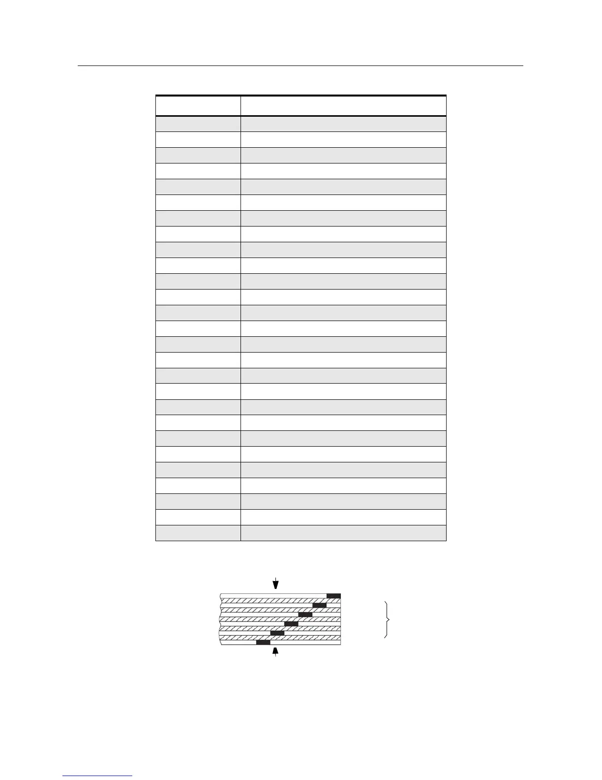
5.1 Six Layer Circuit Board
Figure 1-1. Six-Layer Circuit Board: Copper Steps in Layer Sequence
Name Description
USWB+ Unswitched Battery Voltage (always on)
5V 5 volts (regulated)
5R 5 volts in RX mode only
5T 5 volts in TX mode only
RESET Low-line reset signal from U320 to uP
D3_3V Digital 3.3 volts (regulated)
3V Analog 3 volts (regulated)
TX_ENA Transmit enable signal from uP to transmitter
PWR_SET DC voltage from ASFIC to TX power control
DEMOD RX audio from backend to ASFIC
BW_SEL Backend filter BW select from ASFIC
RSSI RX signal strength indication from IFIC to uP
IF_IN/OUT 44.85 MHz from 1st mixer to high IF filter
RF_IN/OUT RX signal from antenna switch to front end
MOD OUT/IN TX modulation from ASFIC to synthesizer
16_8_MHZ Ref osc signal from synthesizer to ASFIC
SYNTH_CS Synthesizer chip select from uP
SPI_CLK Serial clock from uP
SPI_DATA_OUT Serial data from uP
LOCK Lock detect indication from synth to uP
PRESC VCO freq feedback from VCOBIC to synth
V_STEER Steering line voltage from synth to VCO's
V_SF Super-filtered 4.5 volts from synth to VCOBIC
VCO_MOD TX modulation from ASFIC to synthesizer
TRB TX/RX control from synth to VCOBIC
RX_INJ Buffered RX VCO output to RX 1st mixer
TX_INJ TX VCO output to transmitter input
LAYER 1 (L1)
LAYER 2 (L2)
LAYER 3 (L3)
LAYER 4 (L4)
LAYER 5 (L5)
LAYER 6 (L6)
INNER LAYERS
SIDE 1
SIDE 2
 Loading...