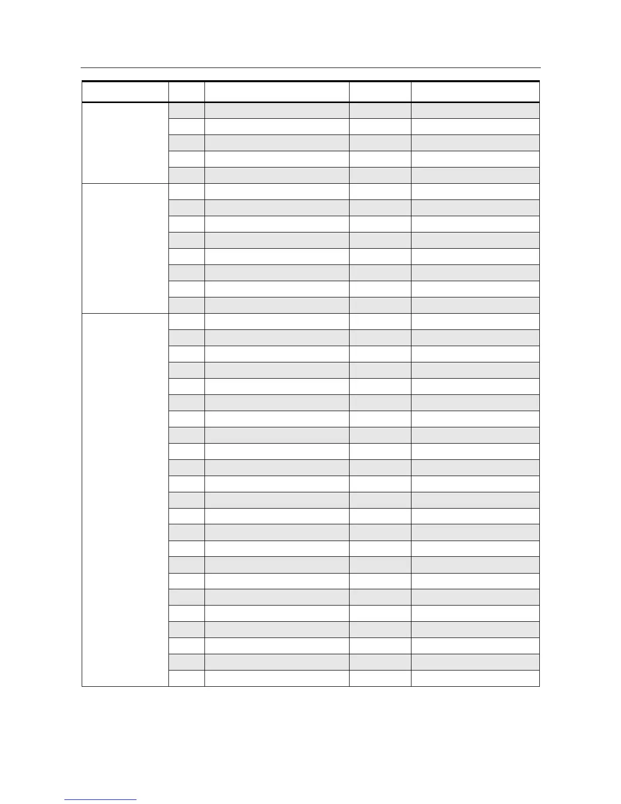
Troubleshooting Table for Board and IC Signals 2-7
U110
RF Power Amp
1 RF input 0 (TX mode)
2 Vgg (gate bias) 2.65 (typ) (TX mode)
3 Vdd 6.59 (TX mode)
4 RF output -- Do not measure
5 Ground GND
U150
Dual Opamp
1 Unit 1 output 4.20 (typ) (TX mode)
2 Unit 1 (-) input 2.39 (typ) (TX mode)
3 Unit 1 (+) input 2.39 (typ) (TX mode)
4 Ground GND
5 Unit 2 (+) input 3.30 (typ) (TX mode)
6 Unit 2 (-) input 3.35 (typ) (TX mode)
7 Unit 2 output 2.23 (typ) (TX mode)
8 Vcc 6.79 (TX mode)
U201
Freq Synthesizer
1 AUX2 output (NU) 0
2 AUX3 output (TRB) 0.03 To U251-19 (RX mode)
3 AUX4 output (NU) 0
4 Lock detect output 2.98 To U401-56
5PD Vdd 2.98
6 Digital ground GND
7 Serial data input 3.23
8 Serial clock input 0
9 Synth chip select 3.23 From U401-47
10 Modulation input 1.50 From U451-40
11 VMULT4 (NU) 2.98
12 VMULT3 (NU) 0
13 VRO 4.96
14 VMULT2 1.49
15 VMULT1 1.49
16 INDMULT (NU) 0
17 NC1 0
18 Ref select (NU) 0
19 Buffered 16.8 MHz out 1.54
20 Analog Vdd 3.00
21 V bypass (NU) 1.55
22 Analog ground GND
23 Ref osc XTAL1 2.07
IC Designator Pin Pin Function DC Voltage Comments (Condition)
 Loading...