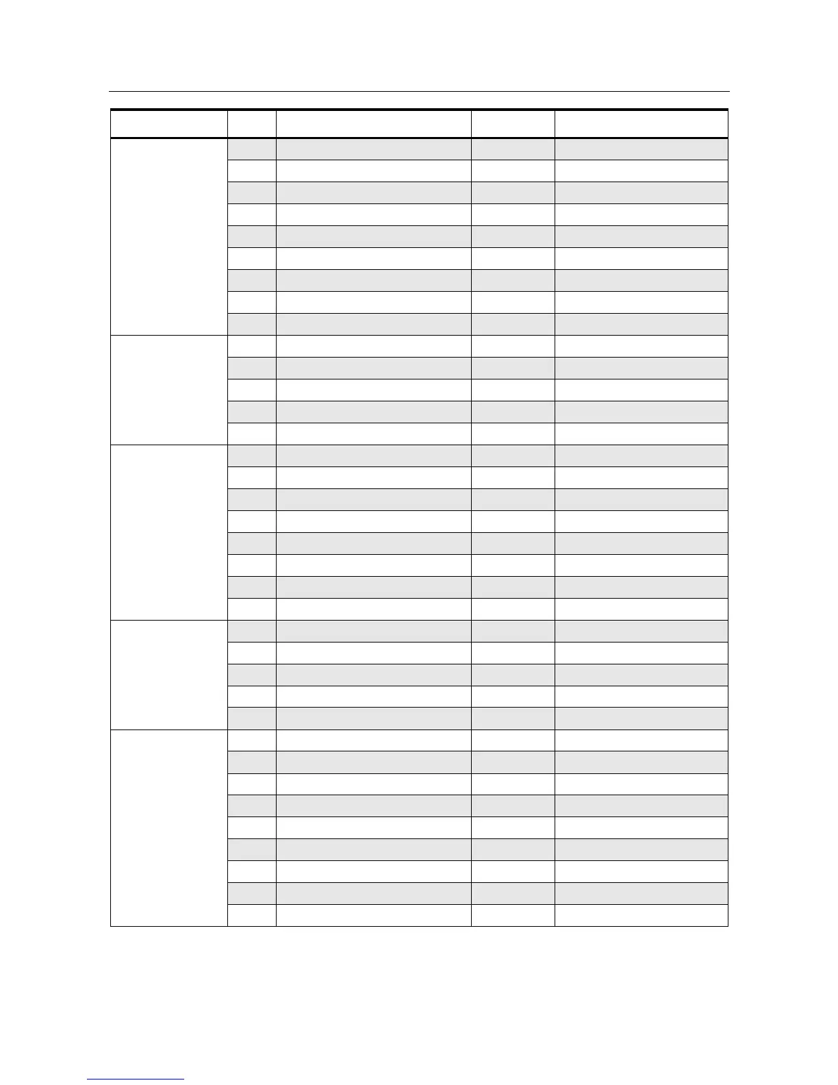
Troubleshooting Table for Board and IC Signals 2-9
U251
VCO / Buffer
12 Prescaler output 2.26
13 TX switch output (NU) 0.06
14 Vcc_BUFFERS 3.00
15 TX VCO emitter 0 (RX mode)
16 TX VCO base 0 (RX mode)
17 GND_LOGIC GND
18 Vcc_LOGIC 3.00
19 TRB input 0.03 From U201-2 (RX mode)
20 FLIP input GND
U310
5V Regulator
1 Vin 7.48
2 Ground GND
3 Control input 7.48
4 Bypass capacitor 1.26
5 Vout 4.96
U320
3.3V Regulator
1 Ground GND
2 Feedback 1.23
3 Tap (NU) 0
4 Vin 7.48
5 Vout 3.23
6 Sense (NU) 0
7 Error (reset output) 3.20
8 Shutdown input 7.48
U330
3V Regulator
1 Vin 7.48
2 Ground GND
3 Control input 7.48
4 Bypass capacitor 1.26
5 Vout 3.00
U401
Microprocessor
1 PD4_SCK serial clock input 0
2 PD5_SS 3.23 ASFIC chip select
3 PD6_VLIN 3.23 EEPROM chip select
4 PG7_R_W 3.21
5PG6_AS 3.23
6 PG0_XA13 3.23
7 PB7_ADDR15 0.026
8 PB6_ADDR14 0.028
9 PB3_ADDR11 3.06
IC Designator Pin Pin Function DC Voltage Comments (Condition)

 Loading...