Frequency Generation Circuitry 1-9
5.0 Frequency Generation Circuitry
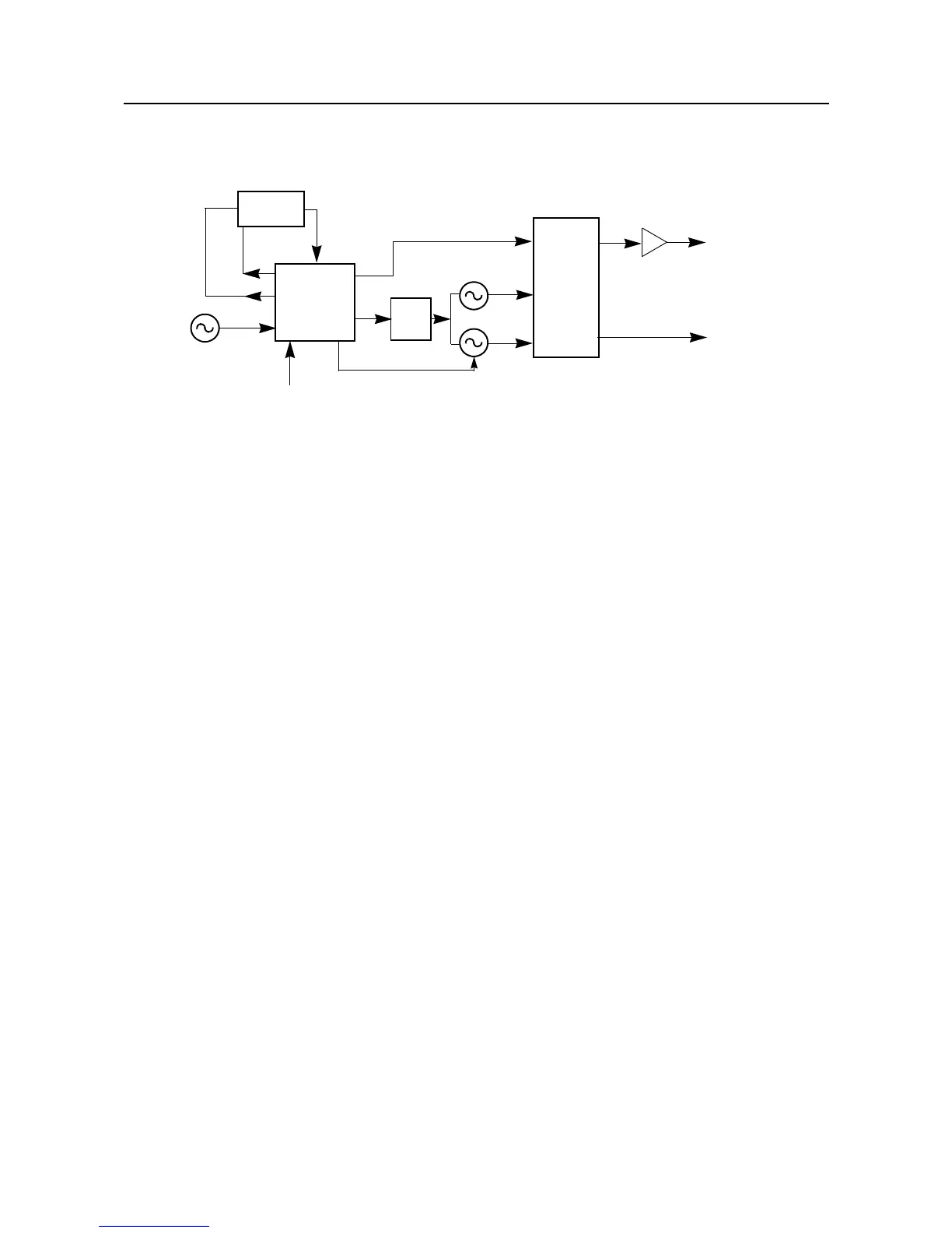
The Frequency Generation Circuitry is composed of two main ICs, the Fractional-N synthesizer
(U3701), and the VCO/Buffer IC (U3801). Designed in conjunction to maximize compatibility, the
two ICs provide many of the functions that normally would require additional circuitry. The
synthesizer block diagram illustrates the interconnect and support circuitry used in the region. Refer
to the relevant schematics for the reference designators.
The synthesizer is powered by regulated 5V and 3.3V which come from U3711 and U3201
respectively. The synthesizer in turn generates a superfiltered 4.5V which powers U3801.
In addition to the VCO, the synthesizer must interface with the logic and ASFIC circuitry.
Programming for the synthesizer is accomplished through the data , clock and chip select lines from
the microprocessor. A 3.3V dc signal from synthesizer lock detect line indicates to the
microprocessor that the synthesizer is locked.
Transmit modulation from the ASFIC is supplied to pin10 of U3701. Internally the audio is digitized
by the Fractional-N and applied to the loop divider to provide the low-port modulation. The audio
runs through an internal attenuator for modulation balancing purposes before going out to the VCO.
5.1 Synthesizer
The Fractional-N Synthesizer uses a 16.8MHz crystal (Y3761) to provide a reference for the
system. The LVFractN IC (U3701) further divides this to 2.1MHz, 2.225MHz, and 2.4MHz as
reference frequencies. Together with C3761, C3762, C3763, R3761 and D3761 , they build up the
reference oscillator which is capable of 2.5ppm stability over temperatures of -30 to 85°C. It also
provides 16.8MHz at pin 19 of U3701 to be used by ASFIC and LVZIF.
The loop filter which consist of C3721, C3722, R3721, R3722 and R3723 provides the necessary
dc steering voltage for the VCO and determines the amount of noise and spur passing through .
In achieving fast locking for the synthesizer, an internal adapt charge pump provides higher current
at pin 45 of U3701 to put synthesizer within the lock range. The required frequency is then locked by
normal mode charge pump at pin 43.
Figure 5-1 Frequency Generation Unit Block Diagram
Voltage
Multiplier
Synthesizer
U3701
Loop
Filter
VCOBIC
U3801
To
Mixer
To
PA Driver
VCP
Vmult1
Aux3
MOD Out
Modulating
Signal
Vmult2
Rx VCO Circuit
Tx VCO
TRB
16.8 MHz
Ref. Osc.
Rx Out
Tx Out
Circuit
 Loading...