Low Band, 800 MHz, PassPort & 900 MHz Theory of Operation: Introduction 7-1
Chapter 7 Low Band, 800 MHz, PassPort & 900 MHz
Theory of Operation
7.1 Introduction
This chapter provides a detailed theory of operation for the radio components. Schematic diagrams
for the circuits described in the following paragraphs are located in Figures 9-238 through 9-284.
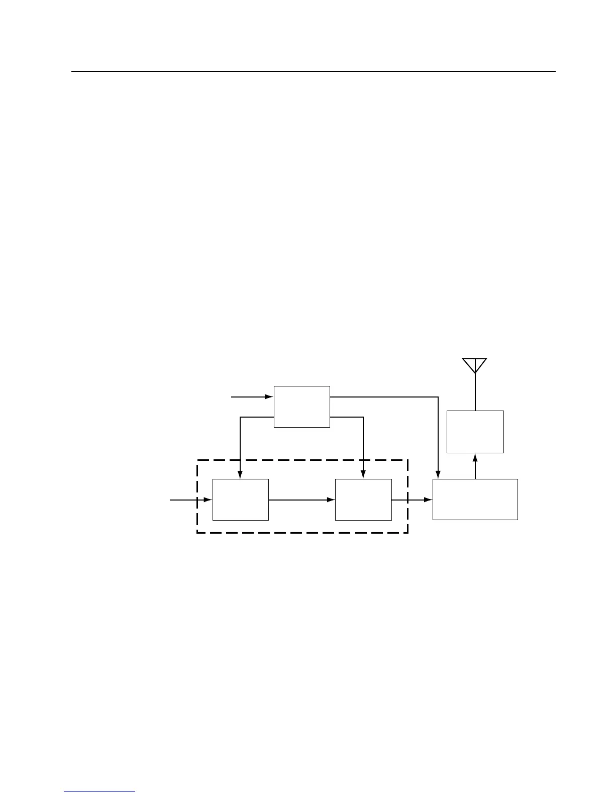
7.2 Low Band Transmitter
The low band transmitter consists of the following basic circuits as shown in Figure 7-1.
• Power amplifier (PA).
• Antenna switch/harmonic filter.
• Antenna matching network.
• Power control integrated circuit (PCIC).
Figure 7-1. Low Band Transmitter Block Diagram
7.2.1 Power Amplifier (PA)
The PA consists of two LDMOS devices:
• PA driver, U101.
• PA final stage, Q100.
The LDMOS driver (U101) provides 2-stage amplification using a supply voltage of 7.3V. The
amplifier is capable of supplying an output power of 0.3 W (pins 6 and 7) with an input signal of 2mW
at (pin16). The current drain is typically 120 mA while operating in the frequency range of
29.7–50 MHz. The power output of this stage is varied by the power control loop which controls the
voltage on pin 1.
PCIC
PA
Driver
Antenna Switch
Harmonic Filter
PA Final
Stage
Vcontrol
SPI Bus
Gate Bias
Antenna Switch Bias
Antenna
Matching
Network
rom VCO
Power Amplifier (PA)
 Loading...