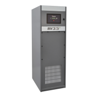
NV5/NV3.5 Troubleshooting Manual Detailed Circuit Descriptions
Issue 3.2 2014-12-10 Page 2-3
Digital outputs
Up to 24 digital outputs can be connected to terminal blocks J3, J4, J5 and J6. You can define these
digital outputs (alarm or status) using the advanced user interface (AUI). Each provides a negative
logic (current-sink-to-ground) output when a ‘true’ (alarm condition or active status) exists. The
outputs provide an open collector during logic 'false' conditions (non-alarm or non-active status
condition) and have no influence on the external monitoring circuit. Each monitoring circuit must
present impedance between the switching device and a positive dc voltage source that results in a
current flow of not more than 30 mA. Each circuit's positive voltage source must not exceed 28 V dc.
A +15 V supply is available for use by the remote monitoring circuits on J1-34 or J1-35 (ground on
J1-36 or J1-37). Bi-position shorting jumpers E1 through E24 allow you to connect each digital
output to a STATUS (green) or ALARM (red) LED, depending on its function. The outputs can also
be labelled according to their function.
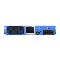
RF power module (NAA56/01D)
See electrical schematics Figures SD-22 through SD-27.
Each RF power module (1 and 2) provides up to 2750 W (for NV5) or 2062.5 W (for NV3.5) of RF
output power and is comprised of an IPA PA PWB (A9), eight PA PWBs (A1 through A8), a power
module interface PWB (A10), a module splitter PWB (A11) and a combiner PWB (A12). Cooling air
for the module is provided by six internal fans (B1 through B6).
An RF Drive output from the RF drive stage is applied to each RF power module via its power
module interface PWB (A10). Within each RF power module, the RF drive signal is amplified
through an IPA PA and then split to drive the module's eight PAs. The IPA Volts input from the
associated power supply module control the RF output of the IPA PA. The PA Volts inputs from the
associated power supply modules control the RF output of the eight PAs. The RF power module
receives alarm signals (PS Temp, PS Fail and PS AC Fail) from the ac-dc power stage, which, when
active, inhibit the PAs. The RF power module also provides a Pwr Supply Inhibit signal to the ac-dc
power stage, which, when active, inhibits the associated switching power supply. A PA V Sample and
IPA V Sample from each RF power module is applied to the control/monitor stage. The control/
monitor stage supplies a PA Volts Inhibit signal, which controls the PA outputs of the RF power
module.
Power amplifier PWBs
See Figures SD-22 and SD-24. Each power amplifier PWB [IPA (A9) and PA (A1 through A8)]
contains an identical, broadband, push-pull, RF power amplifier (PA). Each PA provides 375 W
(nominal) of RF power in the FM band (87.5 to 108 MHz). The RF Drive, PA V and Bias voltage are
provided by the power module interface PWB (A10).