Copyright © Neoway Technology Co., Ltd. All rights reserved.
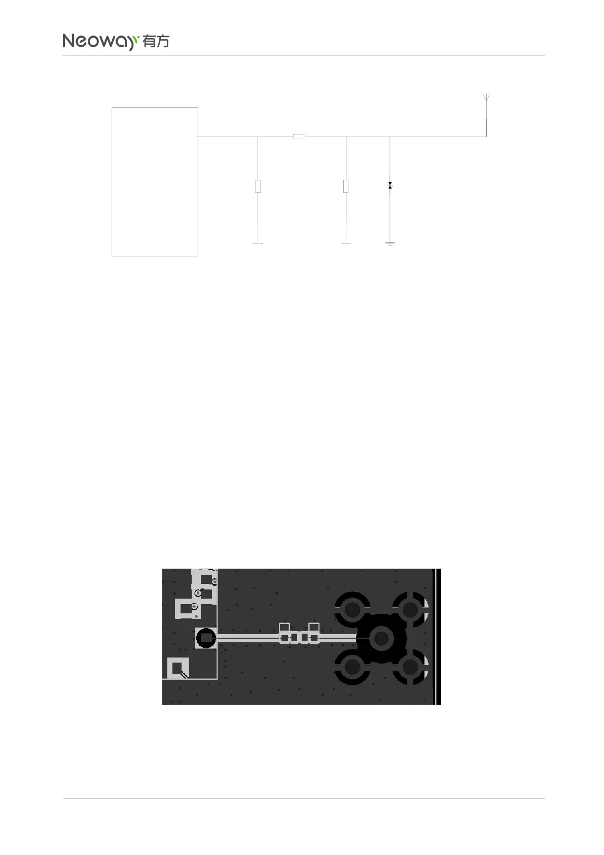
Figure 3-18 Pi network
Schematic Design Guidelines
Element components in the above figures are capacitors, inductors, and 0 Ω resistors. Place
these RLC components as close to the antenna interface as possible.
Add an ESD protector if the antenna might generate static electricity. The protector can be a TVS
diode with a junction capacitance of lower than 0.5 pF. Ensure that the reverse breakdown
voltage of the TVS is higher than 15 V.
PCB Design Guidelines
Pour the ground around RF connector. Dig as many vias as possible on the ground plane to
ensure lowest ground impedance.
The traces between N21 and the antenna connector, should be as short as possible. Control the
trace impedance to 50Ω.
If customers adopt SMA connector, big RF solder pad might result in great parasitic capacitance,
which will affect the antenna performance. Remove the copper on the first and second layers
under the RF solder pad.
Figure 3-19 Recommended RF PCB design
On the PCB, keep the RF signals and components far away from high-speed circuits, power
supplies, transformers, great inductors, the clock circuit, etc.

 Loading...