Do you have a question about the NXP Semiconductors S32K148 and is the answer not in the manual?
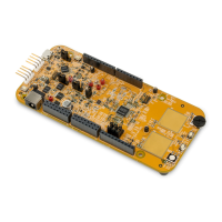
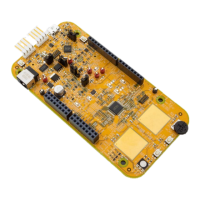
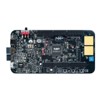
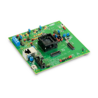
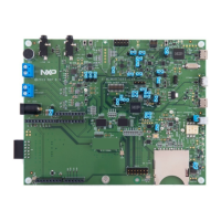
Key features and capabilities of the S32K148 T-BOX RDB.
Datasheets and references for main chips and modules.
Details on the S32K148 T-BOX RDB software package and its contents.
Maps Arduino UNO header pins to specific ports and signals.
Maps external modules and MCU pins to connectors on the board.
Signal routing, wiring harness, and pin descriptions for the 23-pin ECU connector.
Configuration options for power supply jumpers on the board.
Configuration options for LIN and RTC clock jumpers.
Instructions for using Ethernet and QSPI, including resistor configuration.
Steps to power up the board and connect the debugger for initial setup.
Guide to creating new projects using S32 Design Studio.
Fundamental concepts and steps for debugging in S32DS.
Steps to create a specific debug configuration using P&E.
| Processor | ARM Cortex-M4F |
|---|---|
| Core Size | 32-Bit |
| Core Speed | up to 112 MHz |
| Maximum CPU Frequency | 112 MHz |
| Temperature Range | -40°C ~ 125°C |
| Peripherals | DMA, PWM, RTC |
| Program Memory Type | Flash |
| Communication Interfaces | CAN, I2C, SPI, UART |
| Operating Voltage | 2.7V to 5.5V |