EasyManua.ls Logo

Onkyo FR-155 - User Manual

Onkyo FR-155
48 pages
To Next Page IconTo Next Page
Loading...
FR-155
Ref. No. 3662
MODEL FR-155
092000
CD/MD TUNER AMPLIFIER
Silver model
UDT
120V AC, 60Hz
UGT
220 -230V AC, 50/60Hz
SAFETY-RELATED COMPONENT WARNING!!
COMPONENTS IDENTIFIED BY MARK ON THE
SCHEMATIC DIAGRAM AND IN THE PARTS LIST ARE
CRITICAL FOR RISK OF FIRE AND ELECTRIC SHOCK.
REPLACE THESE COMPONENTS WITH ONKYO
PARTS WHOSE PART NUMBERS APPEAR AS SHOWN
IN THIS MANUAL.
MAKE LEAKAGE-CURRENT OR RESISTANCE
MEASUREMENTS TO DETERMINE THAT EXPOSED
PARTS ARE ACCEPTABLY INSULATED FROM THE
SUPPLY CIRCUIT BEFORE RETURNING THE
APPLIANCE TO THE CUSTOMER.
TABLE OF CONTENTS
Specifications -----------------------------------------------------------
Caution on replacement of optical pickup ---------------------------
Protection of eyes from laser beam during servicing ---------------
Laser Warning Label----------------------------------------------------
Service procedures -----------------------------------------------------
Front panel view --------------------------------------------------------
Connecting to Other Components------------------------------------
Remote controller -------------------------------------------------------
Setting the day of the Week and the Time----------------------------
IC Block diagram and descriptions -----------------------------------
Microprocessor Connection Diagram---------------------------------
Microprocessor Terminal Description--------------------------------
Operation of the Microprocessor--------------------------------------
MD Mechanism Exploded view-------------------------------------
MD Mechanism Disassembly ----------------------------------------
MD Mechanism Reassembly ----------------------------------------
MD Adjustment Procedures ------------------------------------------
MD Mount View / Messages--------------------------------------------
CD Mechanism Exploded View ---------------------------------------
CD Adjustment Procdedure-------------------------------------------
Clock Adjustment Procdedure-----------------------------------------
Handling of Pickup-----------------------------------------------------
Chassis Exploded View Parts List------------------------------------
Chassis Exploded View ------------------------------------------------
Block Diagram----------------------------------------------------------
Block Diagram (Power Supply Section)------------------------------
Schematic Diagram (Amplifire Section)-----------------------------
Printed Circuit Board View 1------------------------------------------
Schematic Diagram (CD&Microprocessor Section)----------------
Printed Circuit Board View 2------------------------------------------
Schematic Diagram (Power Supply Section)-----------------------
Printed Circuit Board View 3------------------------------------------
Printed Circuit Board View Parts List--------------------------------
Wiring View-------------------------------------------------------------
Packing View Parts List------------------------------------------------
2
2
3
3
3
4
5
6
6
7
15
16
17
18~19
20,21
22
23~25
26
27,28
29
30
31
32
33
35
37
39
41
43
45
47
49
51~54
55
57
Question and Answer IconNeed help?

Do you have a question about the Onkyo FR-155 and is the answer not in the manual?

Onkyo FR-155 Specifications

General IconGeneral
BrandOnkyo
ModelFR-155
CategoryAmplifier
LanguageEnglish

Summary

Safety-Related Component Warning

Product Specifications and Precautions

Key Product Specifications

Details on general, amplifier, CD, MD, and tuner performance parameters.

Optical Pickup Replacement Precautions

Safety warnings and general precautions for handling the optical pickup.

Laser Safety During Servicing

Laser Diode Properties

Technical specifications including material, wavelength, and output of the laser diode.

Laser Warning Labels and Service Procedures

Information on affixed laser warning labels and essential service procedures.

Front Panel Overview

Front Panel Controls and Indicators

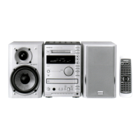
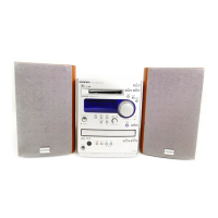
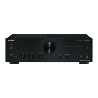
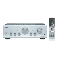
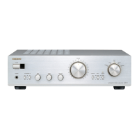
Diagram and labels for all controls, buttons, and display elements on the front panel.

Display Indicator Explanations

Explanation of various indicators shown on the unit's multi-purpose display.

External Device Connectivity

Connecting Various External Devices

Instructions for connecting cassette decks, CD recorders, MD players, DVD players, and subwoofers.

Remote Controller and Clock Settings

Remote Controller Layout

Diagram and labels for all buttons on the remote controller.

Setting the Day and Time

Step-by-step guide to set the unit's clock and day of the week.

Integrated Circuit (IC) Block Diagrams

Q401: TC9273 N-004 Analog Function Switch

Functional overview and pinout for the TC9273N analog switch IC.

Q103, Q181: TA7291 S Motor Driver

Functional overview and pinout for the TA7291S motor driver IC.

Q447: TC9162 AN Analog Function Switch

Functional overview and pinout for the TC9162AN analog switch IC.

CD Digital Signal Processor Block Diagram

Q351: CXD2589 Q Functional Overview

Functional overview of the CXD2589Q CD digital signal processor.

CXD2589 Q Pin Descriptions

CXD2589 Q Pin Definitions (1-42)

Detailed pin numbers, I/O, and descriptions for the CXD2589Q IC.

CXD2589 Q Pin Definitions (43-80)

Detailed pin numbers, I/O, and descriptions for the CXD2589Q IC.

RF Signal Processing Servo Amplifier Block Diagram

Q101: CXA1992 BR Functional Overview

Functional overview of the CXA1992BR RF signal processing servo amplifier.

CXA1992 BR Pin Descriptions

CXA1992 BR Pin Definitions (1-26)

Detailed pin numbers, I/O, and descriptions for the CXA1992BR IC.

CXA1992 BR Pin Definitions (27-52)

Detailed pin numbers, I/O, and descriptions for the CXA1992BR IC.

CD 4-Channel BTL Driver & RDS Decoder Diagrams

Q102: LA6541 D Pin Descriptions

Pinout and function descriptions for the LA6541D 4-channel BTL driver.

Q171: BU1923 RDS Decoder

Pinout and function descriptions for the BU1923 RDS decoder.

FL Tube Driver Block Diagram and Pins

Q752: M66004 F Functional Overview

Functional overview of the M66004F FL tube driver IC.

Q752: M66004 F Pin Definitions

Pinout and function descriptions for the M66004F FL tube driver IC.

FL Tube Display Patterns and Pin Assignments

Display Mode Patterns

Visual examples of display patterns for various modes and indicators.

Pin Assignment Table

Table mapping pins to specific display segments and functions.

System Microprocessor Connection Diagram

System Component Interconnections

Diagram illustrating connections between the microprocessor and other system blocks.

Microprocessor Terminal Descriptions

Q701: MPD780058 GC Pin Functions (1-40)

Pinout and function descriptions for the MPD780058GC microprocessor.

Q701: MPD780058 GC Pin Functions (41-80)

Pinout and function descriptions for the MPD780058GC microprocessor.

Microprocessor Operation Modes

Energy Save Function Operation

Explanation of how the microprocessor interacts with the energy save function.

Control Logic for Muting Functions

Details on how the microprocessor controls CD, Tuner, and MD mute functions.

Other Operations Control

Control logic for various other operations managed by the microprocessor.

MD Mechanism Exploded View (Part 1)

MD Mechanism Assembly Diagram

Illustrated breakdown of the MD mechanism's upper assembly.

MD Mechanism Parts List (1-35)

List of part numbers and descriptions for MD mechanism components.

MD Mechanism Exploded View (Part 2)

MD Mechanism Assembly Diagram

Illustrated breakdown of the MD mechanism's lower assembly and electronic components.

MD Mechanism Parts List (51-74)

List of part numbers and descriptions for MD mechanism components.

MD Mechanism Disassembly Steps

Disassembly Steps (1-8)

Illustrated guide for the first eight steps of MD mechanism disassembly.

MD Mechanism Disassembly Continued

Disassembly Steps (9-16)

Illustrated guide for disassembly steps nine through sixteen.

MD Mechanism Disassembly and Reassembly

Disassembly Steps (17-20)

Illustrated guide for the final disassembly steps seventeen through twenty.

Reassembly Procedure Notes

Important notes and precautions for reassembling the MD mechanism.

MD Recording Adjustment Procedures

Test Mode Operations

Instructions for entering, operating, and exiting the MD test mode.

Test Mode Selection

List of available test modes and their corresponding display names.

MD Adjustment Precautions and Setup

Laser Adjustment Precautions

Safety warnings and guidelines for checking laser emission.

Adjustment Information and Instruments

Overview of adjustment types, required tools, and test discs.

Temperature Compensation Offset Adjustment

Procedure for adjusting temperature compensation offset.

MD Laser Power and EF Balance Adjustments

Laser Power Check Procedure

Procedure for checking and verifying laser power output.

EF Balance Adjustment Procedure

Procedure for adjusting the EF balance of the optical pickup.

MD Mount Views and Display Messages

MD Mount Board Views

Diagrams showing the layout of components on MD mount boards.

Display Message Explanations

Table explaining various messages displayed by the unit.

CD Mechanism Exploded View (Part 1)

CD Mechanism Assembly Diagram

Illustrated breakdown of the CD mechanism's components.

CD Mechanism Exploded View (Part 2)

CD Mechanism Assembly Diagram

Illustrated breakdown of the CD mechanism's components and parts.

CD Mechanism Parts List

List of part numbers and descriptions for CD mechanism components.

CD Adjustment Procedures

Focus Gain Adjustment

Procedure for adjusting the focus gain on the CD player.

Clock Frequency Adjustment

Clock Frequency Calibration

Procedure for adjusting and calibrating the system clock frequency.

Optical Pickup Handling Precautions

Optical Pickup Work Procedure

Step-by-step guide for safely handling and replacing the optical pickup.

Chassis Exploded View Parts List

Chassis Component List (Ref. No. 1-43)

List of part numbers and descriptions for chassis components.

Chassis Component List (Ref. No. F901-U14)

List of PCB references, connectors, and fuses for the chassis.

Chassis Exploded View Diagram

Chassis Assembly Diagram

Illustrated breakdown of the main chassis assembly and its components.

System Block Diagrams

Selector, Tuner, Acoustic, Power Amp Circuits

Block diagram showing connections for selector, tuner, and acoustic circuits.

Display, Microprocessor, CD Circuits

Block diagram showing connections for display, microprocessor, and CD circuits.

Power Supply and MD Mechanism Circuits

Block diagram showing connections for power supply and MD mechanism.

Power Supply Section Block Diagram

Primary and Power Amplifier Circuits

Block diagram of the primary and power amplifier circuit boards.

Power Supply and Microprocessor Circuits

Block diagram of the power supply and microprocessor circuit boards.

Amplifier Section Schematic Diagram

Amplifier Circuit Schematics

Detailed schematic showing the amplifier circuitry and component connections.

Amplifier Section Schematic Diagram (Continued)

Amplifier Circuit Schematics

Detailed schematic showing the amplifier circuitry and component connections.

CD & Microprocessor Schematic Diagram

CD Mechanism and Microprocessor Connections

Schematic showing connections between the CD mechanism and microprocessor.

Printed Circuit Board Views (Part 2)

U6 Microprocessor & CD Circuit PC Board

Layout diagram for the microprocessor and CD circuit PC board (NADG-6933).

U4 Speaker Terminal PC Board

Layout diagram for the speaker terminal PC board (NAETC-6932).

U12 CD Connector PC Board

Layout diagram for the CD connector PC board (NAETC-6939).

Display & Power Supply Schematic Diagrams

Display Circuit Schematic

Schematic diagram for the display circuit.

Power Supply Circuit Schematic

Schematic diagram for the power supply circuit.

Printed Circuit Board Views (Part 3)

U8 Display Circuit PC Board

Layout diagram for the display circuit PC board (NADIS-6935).

U1 Power Supply Circuit PC Board

Layout diagram for the power supply circuit PC board (NAPS-6928).

U9 Control Switch PC Board

Layout diagram for the control switch PC board (NASW-6936).

U5 Headphone Jack PC Board

Layout diagram for the headphone jack PC board (NAETC-7034).

Printed Circuit Board Parts Lists

Power Supply Circuit Board Parts

List of components for the Power Supply Circuit PC Board (NAPS-6928).

Primary Circuit Board Parts

List of components for the Primary Circuit PC Board (NAPS-6929).

Printed Circuit Board Parts Lists (Continued)

Power Amplifier Circuit Board Parts

List of components for the Power Amplifier Circuit PC Board (NAAF-6930).

Microprocessor and CD Circuit Board Parts

List of components for the Microprocessor and CD Circuit PC Board (NADG-6933).

Acoustic Circuit Board Parts List

Acoustic Circuit Board Components

List of components for the Acoustic Circuit PC Board (NAAF-6934).

Printed Circuit Board Parts Lists (Miscellaneous)

Display, CD Connector, Headphone, Control, Selector Boards

Lists components for display, CD connector, headphone, control, and selector boards.

System Wiring Diagram

Selector, Tuner, Acoustic, Power Amp Circuits Wiring

Wiring diagram for selector, tuner, acoustic, and power amplifier circuits.

Display, Microprocessor, CD, MD Mechanism Wiring

Wiring diagram for display, microprocessor, CD, and MD mechanism circuits.

Power Supply, Speaker Terminal, Headphone Wiring

Wiring diagram for power supply, speaker terminal, and headphone circuits.

Packing View and Parts List

Packing Diagram

Illustrated view of the product's packing configuration.

Packing Parts List

List of all parts and accessories included in the product packaging.

Manufacturer Information

Onkyo Corporation Headquarters

Contact details for ONKYO CORPORATION sales and planning division.

Onkyo U.S.A. Corporation

Contact details for ONKYO U.S.A. CORPORATION.

Onkyo Europe Electronics GmbH

Contact details for ONKYO EUROPE ELECTRONICS GmbH.

Onkyo China Limited

Contact details for ONKYO CHINA LIMITED.

Related product manuals