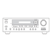
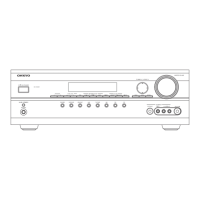
TX-SR502/E/8250/HT-R520
IC BLOCK DIAGRAM AND TERMINAL DESCRIPTIONS-1
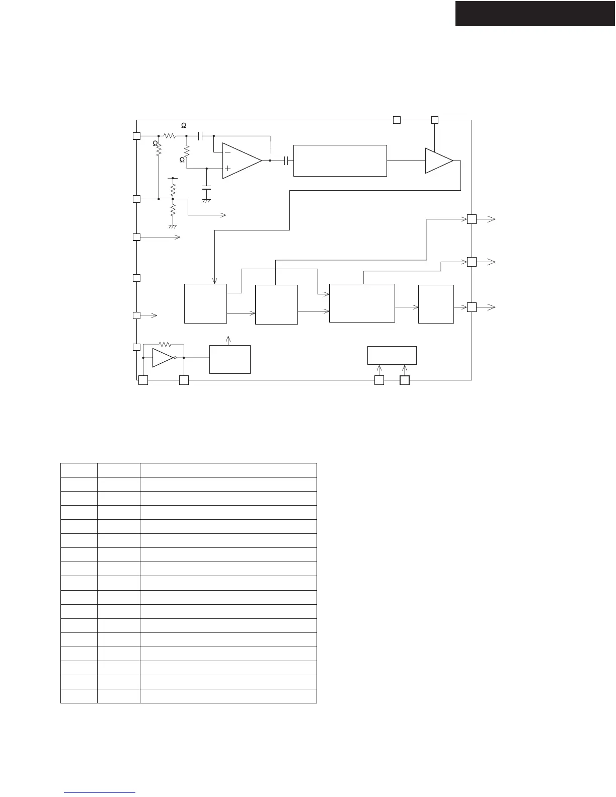
Q181: BU1924FS (RDS decoder)-1
BLOCK DIAGRAM
TERMINAL DESCRIPTION
CMP
VSS3
comparator
8th Switched
capacitor filter
anti-aliasing
filter
100k
120k
100k
MUX
Vref
V
DD1
Analog
Power supply
V
SS1
VDD2
Digital
Power supply
V
SS2
XI
XO
PLL
57kHz
RDS/ARI
PLL
1187.5Hz
Bi-phase
decoder
Measurement
circuit
Differential
decoder
T1 T2
RDATA
QUAL
RCLK
Reference
clock
(4)
(7) (8)
(3)
(16)
(1)
(2)
(5)
(6)
(12)
(11)
(13) (14) (10) (9)
Pin No.
1
6
7
8
2
9
10
3
4
11
12
13
14
15
16
5
Pin name
QUAL
V
SS1
RDATA
T2
T1
Vref
MUX
CMP
VSS2
VDD2
XI
XO
(N.C.)
RCLK
V
DD1
VSS3
Description
Output terminal of demodulator quality signal.
Output terminal of demodulator data.
Input terminal of reference voltage.
Input terminal of composite signal.
Analog power supply.
Analog power supply.
Ground.
Input terminal of comparator.
Input terminal for test mode.
Input terminal for test mode.
Digital power supply.
Digital power supply.
Connect to oscillator.
Connect to oscillator.
---
Output terminal of demodulator clock.
 Loading...