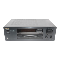
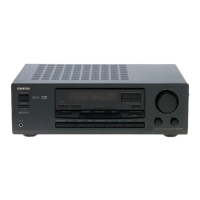
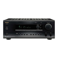
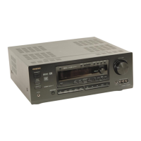
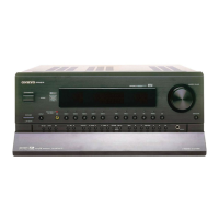
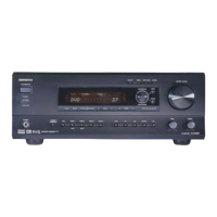
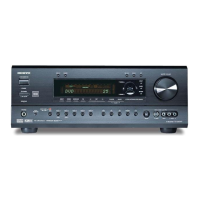
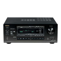
TX-DS494/HT-R490
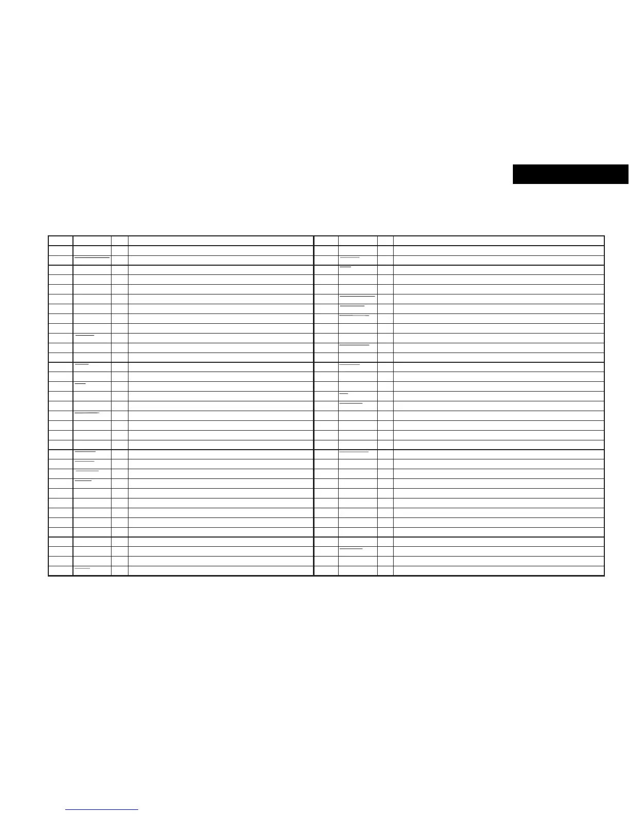
No. Function I/O Description No. Function I/O Description
1 VDD I Power supply terminal. (+5V) 38 RDSSCK I Clock input terminal from RDS decoder.
2 STBY/RECV O STANDBY/RECEIVED inductor control output terminal. 39 REMIN I Signal input terminal from remote sensor.
3 FSWSDO O Data output terminal to function switch ICs. 40 VSS I Power supply terminal (GND).
4 FSWSCK O Clock output terminal to function switch ICs. 41 TUMUT O Muting control output terminal for tuner section.
5 FSWSLT O Latch output terminal to function switch ICs. 42 AMUT O Muting control output terminal for amplifier section.
6 RDSDATA I Data input terminal from RDS decoder. 43 ABOOT/INT I/O AUTOBOOT and INTREQ I/O terminal for DSP(CS4296).
7 SDO O Data output terminal to PLL IC and Master volume IC (TC9482N). 44 KARRST O Not used.
8 SCK O Clock output terminal to PLL IC and Master volume IC (TC9482N). 45 CFGGAIN O Not used.
9 PLLCE O Chip enable output terminal to PLL IC. 46 VDD I Power supply terminal (+5V).
10 RESET I System reset input terminal. 47 GAINCTL O Gain control output terminal.
11 X1 O Ceramic oscillator connection terminals. 48 CODECPD O Power down signal output terminal to CODEC(AK4526).
12 X2 I Connect 5.0MHz ceramic oscillator between the both terminals. 49 DIRPD O Power down signal output terminal to DIR (AK4110).
13 GND I Internal connection terminal.(to GND) 50 DIRCS O Chip enable output terminal to DIR (AK4110).
14 XT2 O Sub system clock output terminal. Not used. 51 BTADRL O Output terminal to set LSB position of address to boot ROM (MX29F002T).
15 XT1 I Sub system clock input terminal. Not used.(to GND) 52 BTADRH O Output terminal to set MSB position of address to boot ROM (MX29F002T).
16 Vdd I Power supply terminal .(+5V) 53 SD I Broadcast detection input terminal.
17 VOL SLT O Latch output terminal to Master volume IC(TC9482N). 54 STEREO I Stereo broadcast detection input terminal.
18 SYSOUT O System code output terminal. 55 RDSSIG I Signal input terminal from RDS decoder.
19 DSPSDI I Data input terminal from DIR(AK4110). 56 SWMUTE O SW Preout muting control output terminal for amplifier section.
20 DSPSDO O Data output terminal to DIR (AK4110),DSP(CS4926,). 57 ERF I ERF Signal input terminal from DIR(AK4110).
21 DSPSCK O Clock output terminal to DIR (AK4110),DSP(CS4926) 58 FS96 O FS96 Signal output terminal to CODEC(AK4526)
22 KARCS O Not used. 59 CODECCS O Not used.
23 DSPCS O Chip enable output terminal to DSP(CS4926). 60 ENC1 I Volume control input terminal.
24 DSPRST O Reset output terminal to DSP(CS4926). 61 ENC2 I Volume control input terminal.
25 AVSS I Power supply terminal.(GND) 62 PROTECT I Detection input terminal for protection circuit.
26 AM9K/10K I Initializing input terminal for AM band step. 63 POWER O Relay control output terminal for power.
27 HPIN I Detection input terminal from headphone.. 64 VCTLB O Video selector control output terminal.
28 MODE I Initializing input terminal of operation mode.. 65 VCTLA O Video selector control output terminal.
29 ECHO I Not used. 66 SPARL O Control output terminal for SPEAKER A relay.
30-33 K3-K0 I Operation key connection terminals. 67 SPBRL O Control output terminal for SPEAKER B relay.
34 AVDD I Power supply terminal.(+5V) 68-78 P17-P7 O Segment output terminals for FL tube.
35 AVREF I Reference voltage terminal. 79 VLOAD Power supply terminal for FL tube.
36 SYSIN I System code input terminal. 80-85 P6-P1 O Segment output terminals for FL tube.
37 POFF I Power failure detection terminal. 86-100 15G-1G O Grid output terminals for FL tube.
MICROPROCESSOR TERMINAL DESCRIPTIUON
Q7001: MPD78P0208GF
 Loading...