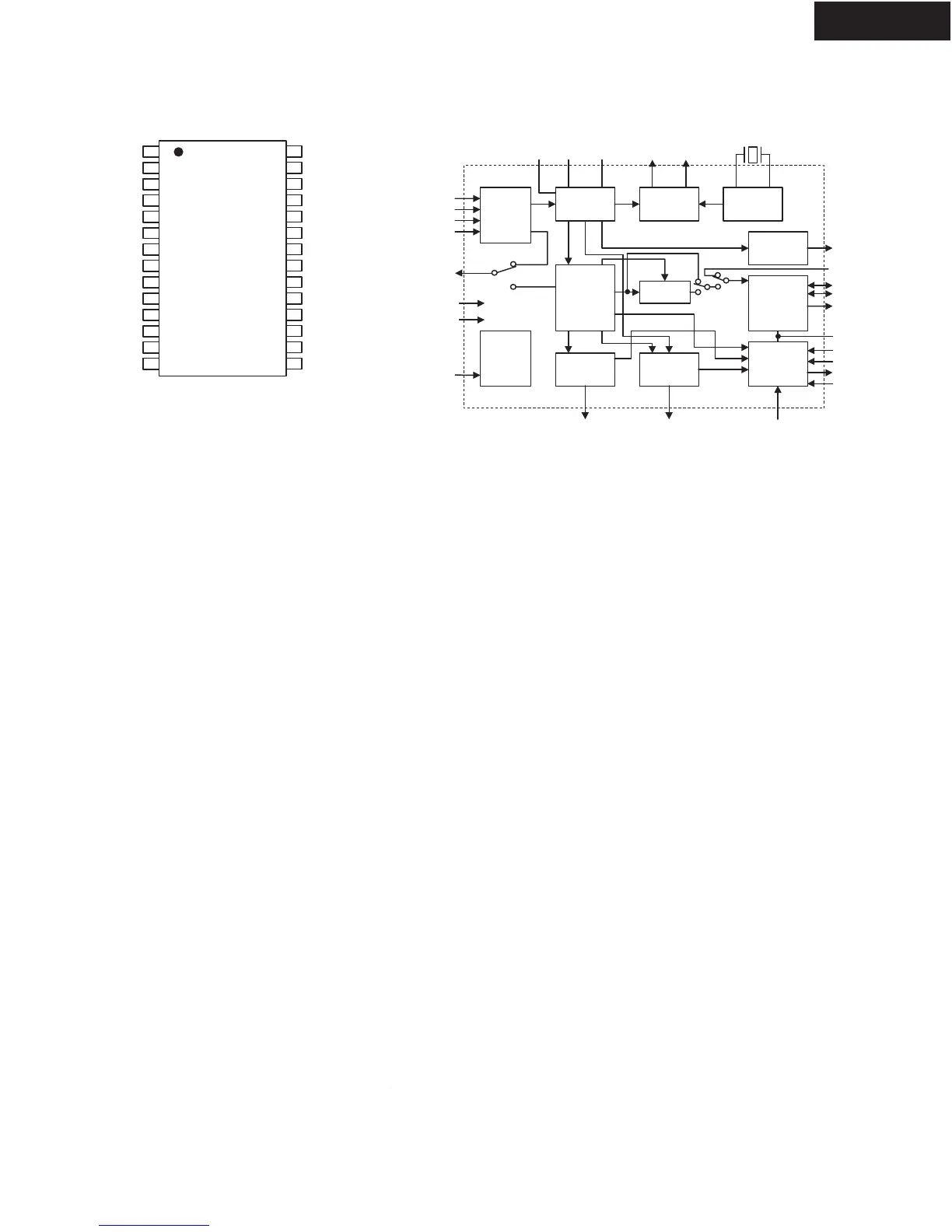
6
5
4
3
2
1
DVDD
DVSS
V/TX
TVDD
XTI
XTO
PDN
7
R
8
Top
View
10
9
AVDD
AVSS
RX1
11
RX2/DIF0
12
13
14
RX3/DIF1
RX4/DIF2
CM0/CDTO
CM1/CDTI
OCKS1/CCLK
OCKS0/CSN
MCKO1
MCKO2
DAUX
BICK
SDTO
LRCK
ERF
FS96
23
24
25
26
27
28
22
21
19
20
18
17
16
15
P/SN
AUTO
No. Pin Name I/O Function
1 DVDD - Digital Power Supply Pin, 3.3V
2 DVSS - Digital Ground Pin
3 TVDD - Input Buffer Power Supply Pin, 3.3V or 5V
V O Validity Flag Output Pin in Parallel Mode
4
TX O Transmit channel (through data) Output Pin in Serial Mode
5 XTI I X'tal Input Pin
6 XTO O X'tal Output Pin
7PDN I
Power-Down Mode Pin
When “L”, the AK4112A is powered-down and reset.
8R -
External Resistor Pin
18k
W
+/-1% resistor to AVSS externall
y.
9 AVDD - Analog Power Supply Pin
10 AVSS - Analog Ground Pin
11 RX1 I
Receiver Channel 1
This channel is selected in Parallel Mode or default of Serial Mode.
DIF0 I Audio Data Interface Format 0 Pin in Parallel Mode
12
RX2 I Receiver Channel 2 in Serial Mode
DIF1 I Audio Data Interface Format 1 Pin in Parallel Mode
13
RX3 I Receiver Channel 3 in Serial Mode
DIF2 I Audio Data Interface Format 2 Pin in Parallel Mode
14
RX4 I Receiver Channel 4 in Serial Mode
15 AUTO O
Non-PCM Detect Pin
“L”: No detect, “H” : Detect
16
P/S
I
Parallel/Serial Select Pin
“L”: Serial Mode, “H”: Parallel Mode
17 FS96 O
96kHz Sampling Detect Pin
(RX Mode) “H” : fs=88.2kHz or more, “L” fs=54kHz or less.
(X’tal Mode) “H” : XFS96=1, “L” : XFS96=0.
18 ERF O
Unlock & Parity Error Output Pin
“ L”: No Error, “H”: Error
19 LRCK I/O Output Channel Clock Pin
20 SDTO O Audio Serial Data Output Pin
21 BICK I/O Audio Serial Data Clock Pin
22 DAUX I Auxiliary Audio Data Input Pin
23 MCK02 O Master Clock #2 Output Pin
24 MCK01 O Master Clock #1 Output Pin
OCKS0 I Output Clock Select 0 Pin in Parallel Mode
25
CSN I Chip Select Pin in Serial Mode
OCKS1 I Output Clock Select 1 Pin in Parallel Mode
26
CCLK I Control Data Clock Pin in Serial Mode
CM1 I Master Clock Operation Mode Pin0 in Parallel Mode
27
CDTI I Control Data Input Pin in Serial Mode
CM0 I
Master Clock Operation Mode Pin1 in Parallel Mode
28
CDTO O Control Data Output Pin in Serial Mode
1: All input pins except internal
pull-down pins should not be left floating.
Input
Selector
S