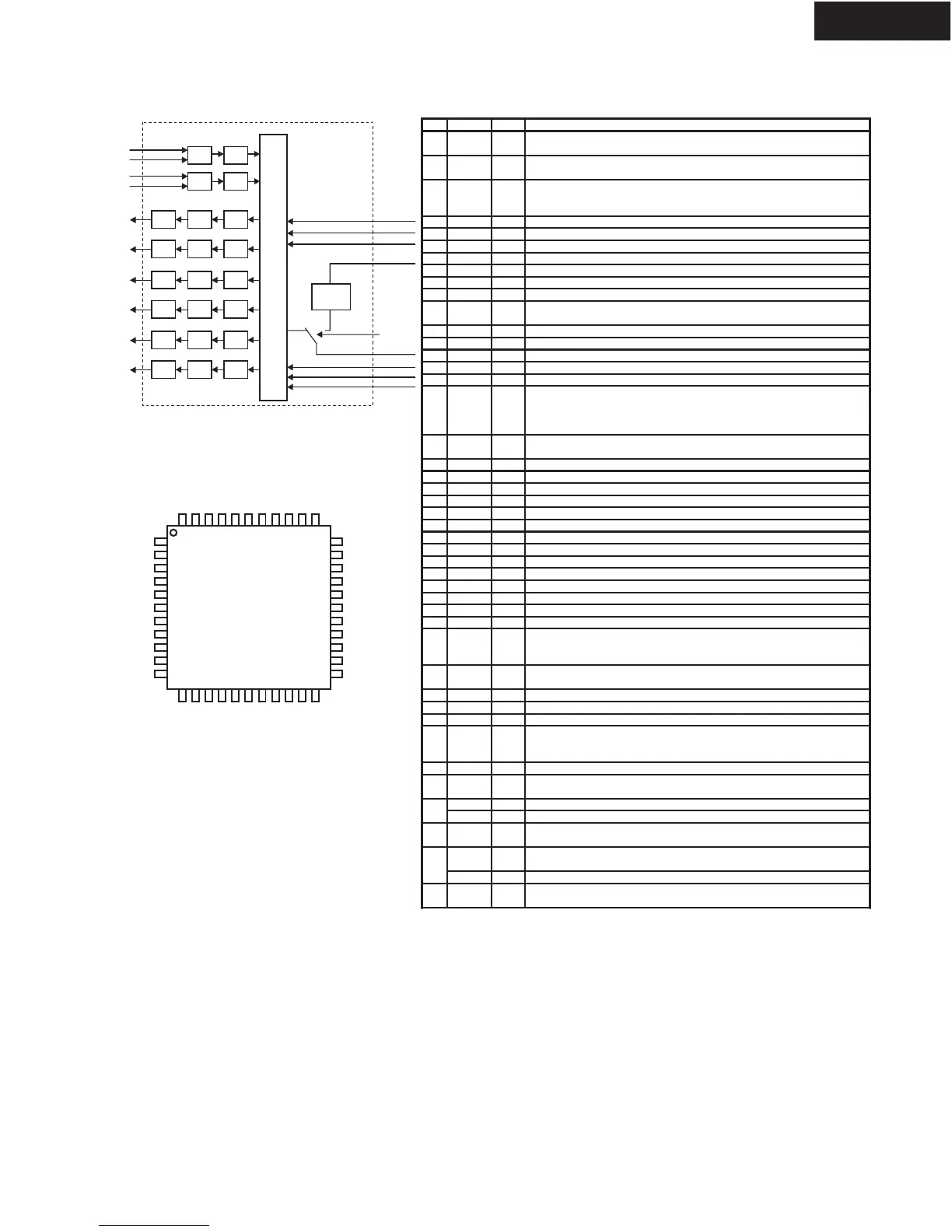
Audio
I/
F
LP
F
LP
F
DA
C
DA
TT
LP
F
DA
C
DA
TT
LP
F
DA
C
DA
TT
LP
FDAC
DA
TT
LP
FDAC
DA
TT
LOUT1
RO
UT1
LOUT
2
RO
UT2
LOUT
3
RO
UT3
DAC
DA
TT
AK4527
ADC
HP
F
AD
C
HP
F
RIN-
RIN+
LIN-
LI
N+
LRCK
BICK
SDTI1
SDTI2
SDTI3
DAUX
SDO
S
MCLK
LRCK
BICK
SDOUT
SDIN1
SDIN2
SDI
N3
MCLK
SDTO
Format
Converter
1
2
3
4
5
6
7
8
9
10
11
12
13
14
15
16
17
18
19
20
21
22
33
32
31
30
29
28
27
26
25
24
23
44
43
42
41
40
39
38
37
36
35
34
AK4527VQ
Top View
SDOS
12C
SMUTE
BICK
LRCK
SDTI1
SDTI2
SDYI3
SDTO
DAUX
DFS
DEM1
DEM0
TVDD
DVDD
DVSS
PDN
ICKS2
ICKS1
ICKS0
CAD1
CAD0
Pin Layout
DZF2
RIN+
RIN-
LIN+
LIN-
ROUT1
LOUT1
ROUT2
LOUT2
ROUT3
LOUT3
LOOP1
LOOP0/CDTI
DF1/CCLK
DIF0/CSN
P/S
MCLK
DZF1
AVSS
AVDD
VREFH
VCOM
PIN/FUNCTION
No. Pin Name I/O Function
1 SDOS I SDTO Source Select Pin (Note 1)
"L" : Internal ADC out
ut
2 I2C I Control Mode Select Pin
This
in should be connected to DVSS.
3 SMUTE I Soft Mute Pin
When this pin goes to "H", soft mute cycle is initialized. When returning to "L",
the out
ut mute releases.
4 BICK I Audio Serial Data Clock Pin
5 LRCK I In
ut Channel Clock Pin
6 SDTI1 I DAC1 Audio Serial Data In
ut Pin
7 SDTI2 I DAC2 Audio Serial Data In
ut Pin
8 SDTI3 I DAC3 Audio Serial Data In
ut Pin
9 SDTO O Audio Serial Data Out
ut Pin
10 DAUX I AUX Audio serial Data In
ut Pin
11 DFS I Double Speed Sampling Mode Pin (Note 1)
"L": Normal S
0V
17 PDN I Power-Down & Reset Pin
When "L", the control registers are reset to defalt state.
If the state of CAD0-1 changes, then the AK4527 must be reset by PDN.
18 ICKS2 I Input Clock Select 2 Pin (Note 1)
This
in should be connected to DVSS.
19 ICKS1 I In
23 LOUT3 O DAC3 Lch Analo
ut Pin
24 ROUT3 O DAC3 Rch Analo
ut Pin
25 LOUT2 O DAC2 Lch Analo
ut Pin
26 ROUT2 O DAC2 Rch Analo
ut Pin
27 LOUT1 O DAC1 Lch Analo
ut Pin
28 ROUT1 O DAC1 Rch Analo
ut Pin
29 LIN- I Lch Analo
ut Pin
30 LIN+ I Lch Analo
ut Pin
31 RIN- I Rch Analo
ut Pin
32 RIN+ I Rch Analo
ut Pin
33 DZF2 O Zero Input Detect 2 Pin (Note 3)
When the input data of the group 1 follow total 8192 LRCK cycles with "0" input
data
s "L" if P/S= "H".
34 VCOM O Common Voltage Output Pin, AVDD/2
Lar
acitor around 2.2 uF is used to reduce
noise.
35 VREFH I Positive Volta
0V
38 DZF1 Zero Input Detect 1 Pin (Note 3)
When the input data of the group 1 follow total 8192 LRCK cycles with "0" input,
data
s "L" if P/S= "H".
39 MCLK I Master Clock In
ut Pin
40 P/S I Parallel/Serial Select Pin
"L": Serial control mode
"H": Parallel control mode
41 DIF0 I Audio Data Interface Format 0 Pin in
arallel control mode
CSN I Chi
Select Pin in serial control mode
42 DIF1 I Audio Data Interface Format 1 Pin in
arallel control mode
CCLK I Control Data Clock Pin in serial control mode
43 LOOP0 I Lookback Mode 0 Pin in
arallel control mode
Enables di
ital look-back from ADC to 3 DACs.
CDTI I Control Data In
ut Pin in serial control mode
44 LOOP1 I Looback Mode 1 Pin
Enables all 3 DAC channels to be in
ut from SDTI1.
Notes: 1.SDOS, SMUTE, DFS, ICKS2-0 and LOOP 1 pins are Ored with register data if P/S="L".
2. DEM1-0 pins are Ored with register data of DEMA1-C0 bits if P/S="L".
DEM1 pin="H" : DEMA1= DEMB1=DEMC1="1"
DEM0 pin="H" : DEMA0= DEMB0=DEMC0="1"
3. The group 1 and 2 can be selected by DZFM2-0 bits if P/S="L".
4. All input pins should not be left floating.
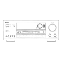
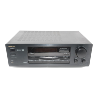
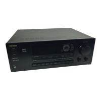
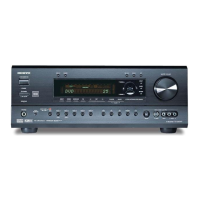
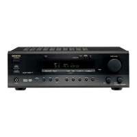
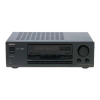
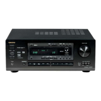
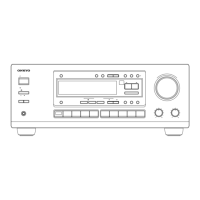
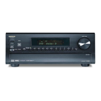
TX-DS595/696
AK4527VQ(24bit 96kHz 6-ch. CODEC)