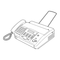
14
KX-FT931LA-B
6.3. Control Section
6.3.1. ASIC (IC1)
This custom IC is used for the general FAX operations.
1. CPU:
This model uses a Z80 equivalent to the CPU operating
at 12 MHz. Most of the peripheral functions are performed
by custom-designed LSIs. Therefore, the CPU only works
for processing the results.
2. RTC:
Real Time Clock
3. DECODER:
Decodes the address.
4. ROM/RAM I/F:
Controls the SELECT signal of ROM or RAM and the
bank switching.
5. CIS I/F:
Controls the document reading.
6. IMAGE DATA RAM:
This memory is programmed into the ASIC and uses 8
KB for the image processing.
7. THERMAL HEAD I/F:
Transmits the recorded data to the thermal head.
8. MOTOR I/F:
Controls the transmission motor which feeds the docu-
ment.
Controls the receiving motor which feeds the recording
paper.
9. OPERATION PANEL I/F:
Serial interface with Operation Panel.
10. I/O PORT:
I/O Port Interface.
11. ANALOGUE UNIT:
Electronic volume for the monitor.
Sends beep tones, etc.
Note*:
This memory is incorporated into the ASIC (IC1) and used for the image processing.
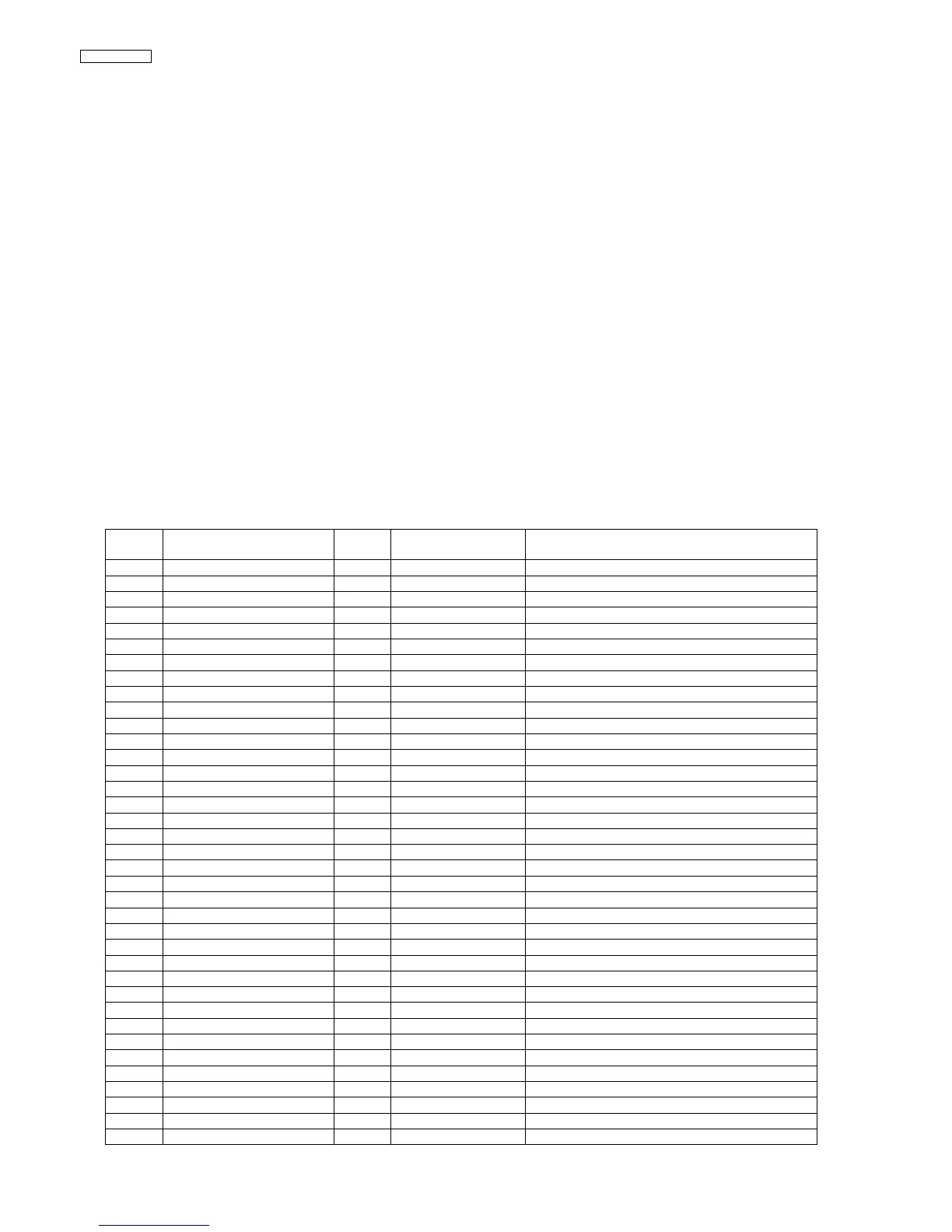
Descriptions of Pin Distribution (IC1)
NO. SIGNAL I/O POWER SUPPLIED
VOLTAGE
DESCRIPTION
1 VSSA GND POWER SOURCE (ANALOG GND)
2 VDDA 3.3 3.3V POWER SOURCE (ANALOG +3.3V)
3 AIN1 A 3.3V CIS IMAGE SIGNAL INPUT (ATN1)
4 AIN2 A 3.3V THERMISTOR TEMPERATURE WATCH INPUT
5 AIN3 A 3.3V LINE VOLTAGE DETECTION SIGNAL INPUT (DCIN)
6 AMON A 3.3V ANALOG SIGNAL MONITOR TERMINAL
7 VSS GND POWER SOURCE (GND)
8 X32OUT O 3.3V/BATT RTC (32.768KHz) CONNECTION
9 X32IN I 3.3V/BATT RTC (32.768KHz) CONNECTION
10 VDD (3.3V / B) ----- POWER SOURCE (+3.3V/LITHIUM BATTERY)
11 XBACEN I 3.3V/BATT BACKUP ENABLE
12 XRAMCS O 3.3V/BATT XRAMCS
13 VDD (3.3V / B) ----- POWER SOURCE(+3.3V / LITHIUM BATTERY)
14 VDD (2.5V/B) ----- POWER SOURCE (+2.5V / LITHIUM BATTERY)
15 FTG O 3.3V SH SIGNAL OUTPUT FOR CIS (FTG)
16 F1 O 3.3V 01 SIGNAL OUTPUT FOR CIS (F1)
17 F2/OP O 3.3V OUTPUT PORT (HEADON)
18 FR/OP O 3.3V OUTPUT PORT (MDMRST)
19 CPC I 3.3V INPUT PORT (CPC)
20 RVN I 3.3V INPUT PORT (PAPER)
21 IRDATXD/IOP I 3.3V INPUT PORT (JAM)
22 IRDARXD/IOP80 O 3.3V OUTPUT PORT (HSTX MUTE)
23 TXD/IOP I 3.3V INPUT PORT (BELL)
24 RXD/IOP I/O 3.3V PORT (TELRXEN)
25 XRTS/IOP I 3.3V INPUT PORT (PSHORT)
26 XCTS/IOP I/O 3.3V PORT (MDMTXEN)
27 VDD (2.5V) ----- POWER SOURCE (+2.5V)
28 TONE1 A 3.3V TONE OUTPUT
29 TONE2 A 3.3V TONE OUTPUT
30 VOLUREF A 3.3V ANALOG REF VOLTAGE
31 VOLUOUT A 3.3V VOLUME OUTPUT
32 VOLUIN A 3.3V VOLUME INPUT
33 XNMI I 3.3V HIGH FIXED
34 FMEMDO/IOP O 3.3V OUTPUT PORT (LED ON)
35 VDD (3.3V) ----- POWER SOURCE (+3.3V)
36 VSS GND POWER SOURCE (GND)
37 VSS GND POWER SOURCE (GND)
 Loading...