45
KX-FT931LA-B
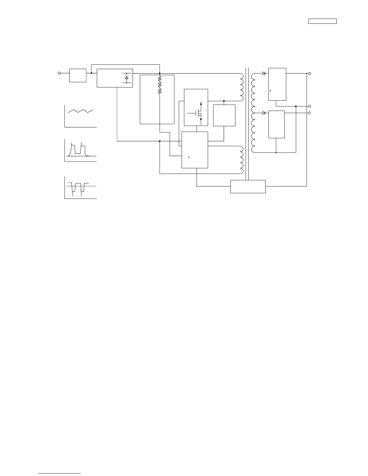
6.12. Power Supply Board Section
This power supply board uses the switching regulator method.
[Input Circuit]
The input current goes into the input rectifier circuit through the filter circuit. The filter circuit decreases the noise voltage and the
noise electric field strength.
[Rectifier Circuit]
The input current is rectified by D10, D11, D12 and D13 and charges C5 to make DC voltage. Then it supplies power to the con-
verter circuit.
[Kick-on voltage circuit]
Bias is applied to the Q1 gate via this circuit when the AC power is turned on and Q1 begins operating.
Input
Circuit
AC
Input
Surge
absorber
circuit
G
H
9~6V
24V
Kick-on
Voltage
Circuit
E
F
GND
Control
Circuit
R2
R3
Converter
Circuit
C
D
6V
Output
Circuit
24V
Output
Circuit
+
-
Rectifier
Circuit
A
B
C5
Error Detecting
Circuit
O.C.L
Q1
A-B Voltage Wave Form
C-D Voltage Wave Form
E-F
G-H
Voltage Wave Form
0
0
0
Block Diagram
R4
Over
voltage
 Loading...