12 IC DATA
12.1. CPU (IC200)
Pin No. Pin Name I/O Description
1 nRDY I CPU bus ready signal
2 nRESET I CPU power on reset input port
3 nCS0 O Chip select 0 for Flash memory
4 nCS1 O Chip select 1 for BUS-M Card
5 nCS4 O Chip select 4 for SRAM
6 nCS5 O Chip select 5 for ASIC
7 nCS6 O Chip select 6 for RTC USB interface SD card interface
8 nBS O CPU bus start signal
9 VDDQ1 Power supply for IO(3.3V)
10 VSSQ1 Power supply for IO(GND)
11 D47/P15 I nFAN_ALM (FAN alarm signal input port)
12 D32/P0 I nCTS1 for debug port
13 VDD1 Power supply for CORE(1.5V)
14 VSS1 Power supply for CORE(GND)
15 D46/P14 O RING_SYNC(Ringer sync signal output port)
16 D33/P1 O nRTS1 for debug port
17 D45/P13 I VBUS(USB Cable detect port )
18 D34/P2 O nDTR2 for RS232C port
19 D44/P12 I nINIT( initialize switch input port)
72
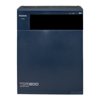
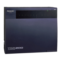
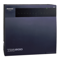
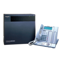
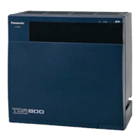
KX-TDA600BX
 Loading...