Pin No. Pin Name I/O Description
151 MD2/RXD2 I CPU Mode Serial interface for RS232C Port
152 nIRL0 I nIRQ_ASIC (Interrupt signal from ASIC)
153 nIRL1 I nIRQ_USB (Interrupt signal from USB controller)
154 nIRL2 I nIRQ_BUSM (Interrupt signal from BUS-M Card)
155 nIRL3 I nDC_ALM (DC Alarm Interrupt signal)
156 NMI I Non Maskable Interrupt (Pull up) NOT USE
157 XTAL2 O Clock oscillator terminal 2 for internal RTC module
158 EXTAL2 I External Clock oscillator terminal 2 for internal RTC module
159 VSS-RTC Power supply for RTC(GND)
160 VDD-RTC Power supply for RTC(3.3V)
161 CA I Hardware standby (Pull up) NOT USE
162 VSS9 Power supply for CORE(GND)
163 VDDQ16 Power supply for IO(3.3V)
164 nCTS2 IO SCIF Data flow control nCS2 for RS232C Port
165 TCLK IO RTC clock output( for factory test use only)
166 MD8/nRTS2 I CPU Mode Data flow control for RS232C Port
167 MD7/TXP I CPU Mode
168 SCK2/nMRRESET I SCIF clock (Pull up) NOT USE
169 VDD7 Power supply for CORE(1.5V)
170 VSS7 Power supply for CORE(GND)
171 A18 O Address Bus [18]
172 A19 O Address Bus [19]
173 A20 O Address Bus [20]
174 A21 O Address Bus [21]
175 A22 O Address Bus [22]
176 A23 O Address Bus [23]
177 VDDQ14 Power supply for IO(3.3V)
178 VSSQ14 Power supply for IO(GND)
179 A24 O Address Bus [24]
180 A25 O Address Bus [25]
181 MD3/nCE2A I CPU Mode
182 MD4/nCE2B I CPU Mode
183 MD5/nRAS2 I CPU Mode
184 DACK0 O DMA Controller Bus acknowledge 0 for USB Controller
185 DACK1 O DMA Controller Bus acknowledge 1 for USB Controller
186 A0 O Address Bus [0]
187 VDDQ15 Power supply for IO(3.3V)
188 VSSQ15 Power supply for IO(GND)
189 A1 O Address Bus [1]
190 STATUS0 O CPU Status (NC) NOT USE
191 STATUS1 O CPU Status (NC) NOT USE
192 MD6/nIOISI6 I CPU Mode
193 nASEBRK/BRKACK IO JTAG Break for debugger
194 TDO O JTAG Data out for debugger
195 VDD8 Power supply for CORE(1.5V)
196 VSS8 Power supply for CORE(GND)
197 TMS I JTAG Mode switch for debugger
198 TCK I JTAG clock for debugger
199 TDI I JTAG test data in port for debugger
200 nTRST I JTAG reset for debugger
201 VDD-PLL2 Power supply for Internal PLL2(3.3V)
202 VDD-PLL2 Power supply for Internal PLL2(GND)
203 VDD-PLL1 Power supply for Internal PLL1(3.3V)
204 VDD-PLL1 Power supply for Internal PLL1(GND)
205 VDD-CPG Power supply for CPG(3.3V)
206 VSS-CPG Power supply for CPG(GND)
207 XTAL O Clock oscillator terminal NC NOT USE
208 EXTAL I External Clock oscillator terminal 16.384MHz(System clock)
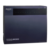
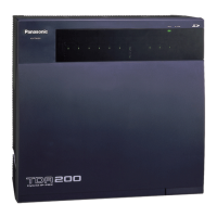
75
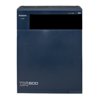
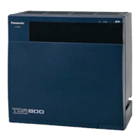
KX-TDA600BX