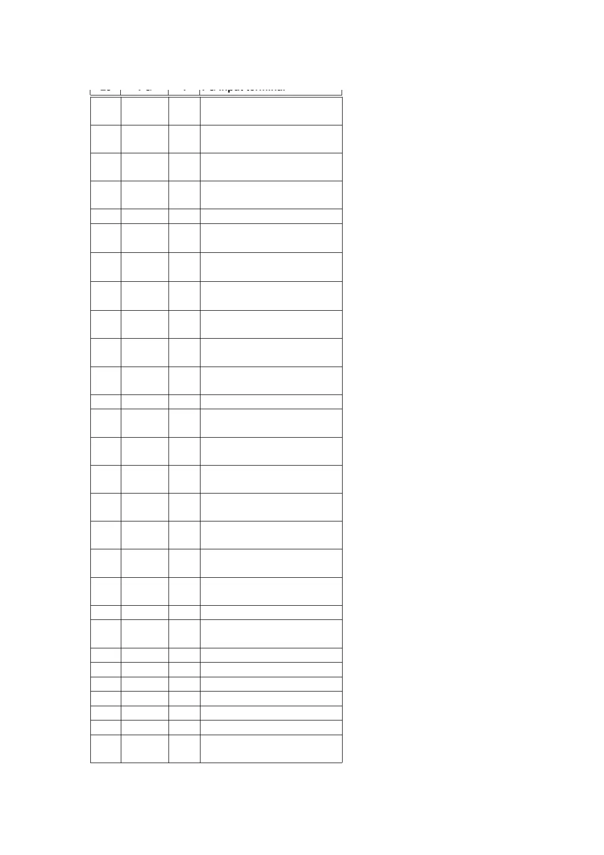
Pin
No.
Mark I/O Function
26 NRECT O Rec/Play switching signal
output terminal
27 IVDD2 — Power supply terminal for I/
O pad
28 IVDD0 — Power supply terminal for I/
O pad
29 DVss0 — GND terminal
30
~32
RAD12
~RAD10
— DRAM address output
terminal (Not used, open)
33
~42
RAD9
~RAD0
O DRAM address output
terminal
43
~46
RDT3
~RDT0
I/O DRAM data input/output
terminal
47 NRAS O DRAM row address strobe
output terminal
48 NCAS O DRAM culum address
strobe output terminal
49 NWE O DRAM write enable output
terminal
50 NRST I Reset signal input terminal
51 SELAD I MSP/MDA,I/F address select
input terminal (“H” Address)
52 SSCK I MSP/MDA,I/F clock input
terminal
53 SSDW I MSP/MDA,I/F write data
input terminal
54 SSDR O MSP/MDA,I/F read data
output terminal
55 MDISY O Leader synchronous signal
output
56 SCTSY O ADIP synchronous noise
output terminal
57 SGSYNC O Frame synchronous signal
output terminal
58 DVDD1 I Power supply terminal
59 IVDD1 — Power supply terminal for I/
O pad
60 DVss1 — GND terminal
61 FS384 O 384 Fs output terminal
62 SCL O Bit clock output terminal
63 SWS O Word clock output terminal
64 SDAP O Audio data output terminal
65 SDAR I Audio data input terminal
66 LRCK I CD word clock input
terminal (Connected to GND)
45