Pin
No.
Mark I/O Function
26 VSS — GND terminal
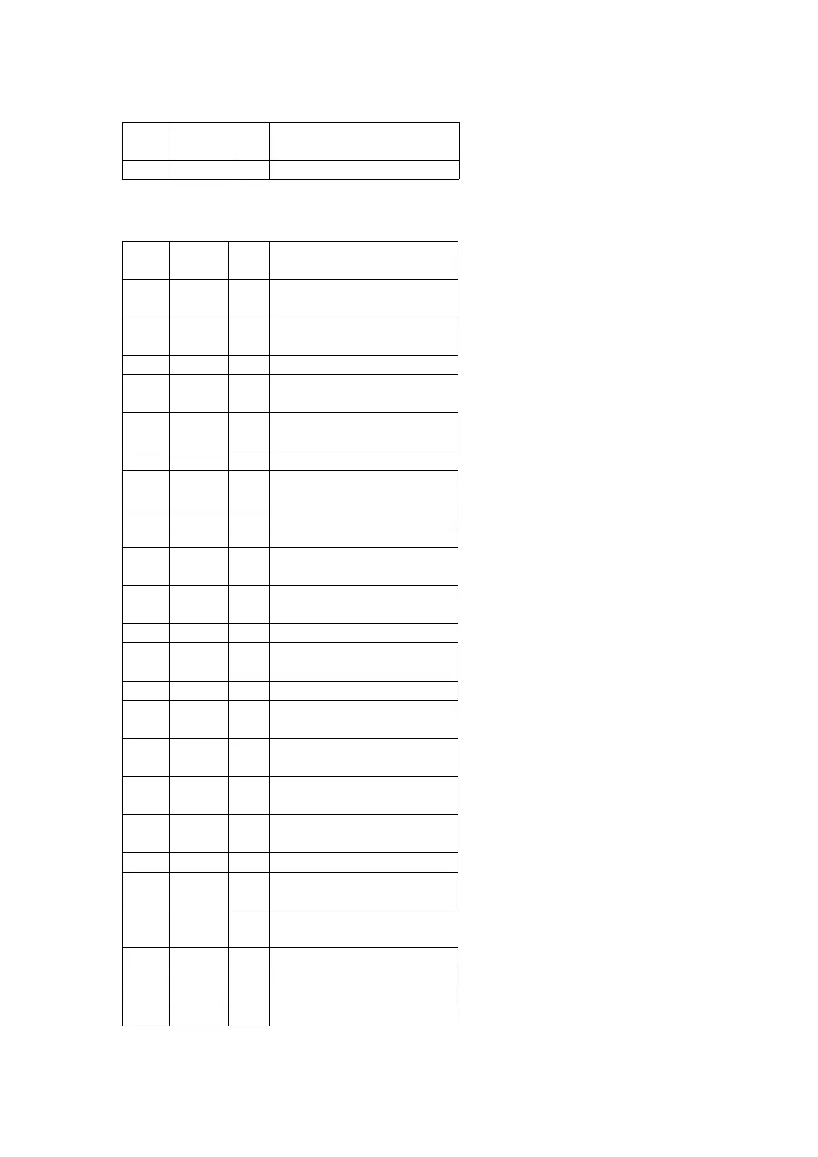
11.6. IC701 (AN8839NSBE2) SERVO AMPLIFIER
Pin
No.
Mark I/O Function
1 PDE I Tracking signal input
terminal 1 (E ch)
2 PDF I Tracking signal input
termianl 2 (F ch)
3 VCC I Power supply connection
4 PDA I Focus signal input termianl
1 (A ch)
5 PDB I Focus signal input terminal
2 (B ch)
6 LPD I Laser PD connection
7 LD O Laser power auto control
output
8 RF O RF signal output
9 RFIN I RF signal input
10 CSBRT I Capacitor for detection
connection
11 CEA I Capacitor connection for
HPF amplifier
12 BDO O BDO output (“H” : drop out)
13 LDON I LD APC input (“H” : ON,
“L” : OFF)
14 GND — Ground connection
15 /RFDET O NRFDET output (“L” :
detection)
16 PDOWN O CROSS output (Track cross
signal output
17 OFTR O Off-track output (“L” : ON
track, “H” : OFF track)
18 N.C. O VDET output (“H” :
Vibration detected)
19 ENV O RF envelope detection
20 N.C. I Not used, connected to
power supply
21 N.C. I Cscillation detect signal
input
22 TEN I Tracking error signal input
23 TEOUT O Tracking error signal output
24 FEOUT O Focus error signal output
25 FEN I Focus error signal input
52