Circuit Descriptions, List of Abbreviations, and IC Data Sheets
EN 86 L04L AA9.
During the first half of the intensity increase, the scan velocity
is increased (thus decreasing the current density by spreading
it on a wider area). During the second half of the intensity
increase, the scan velocity is decreased (increasing the current
density by concentrating it on a smaller area). The increasing
current density transition is sharpened. A decreasing current
density transition is processed in a similar way and is also
sharpened.
In this chassis the SCAVEM signal is different from its
predecessor because the Hercules generates the differential
SCAVEM signal inside the IC.
The supply of the SCAVEM is taken from V_bat through a 1k5
/ 5 W resistor. Compared with the L01.1, this has the advantage
of getting better performance for the pattern with tremendous
SCAVEM current (like V_sweep). In this former chassis,
because the supply was taken from the 200 V through a 8k2 /
5 W resistor, the supply dropped significantly during a large
SCAVEM current. In this chassis, the drop due to the pattern
will be less because of the lower supply voltage impedance.
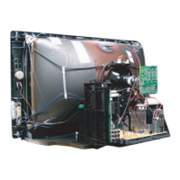
In the Main Board, 1st stage amplification is taken care by 7208
with the pull up resistors (3361, 3387) located in the CRT panel.
TS7361 and TS7362 is the current buffer delivering the current
to the output stage. The diode D6361 is to lightly bias these
transistors, to get rid of the zero crossover of the stage.
After that, the signal is ac-coupled to TS7363 and TS7364
where the emitter resistors (R3364 and R3370) will determine
the final SCAVEM current. TS7363 and TS7364 are biased by
R3363, R3366, R3367 and R3368.
C2387, R3388, R3389, R3365, R3369, C2384, and C2385 are
used for suppressing unwanted oscillations.
The function of TS7376 is to limit the SCAVEM current from
going too high. It basically senses the voltage after R3373 and
clamps the SCAVEM signal through D6367 and C2376.
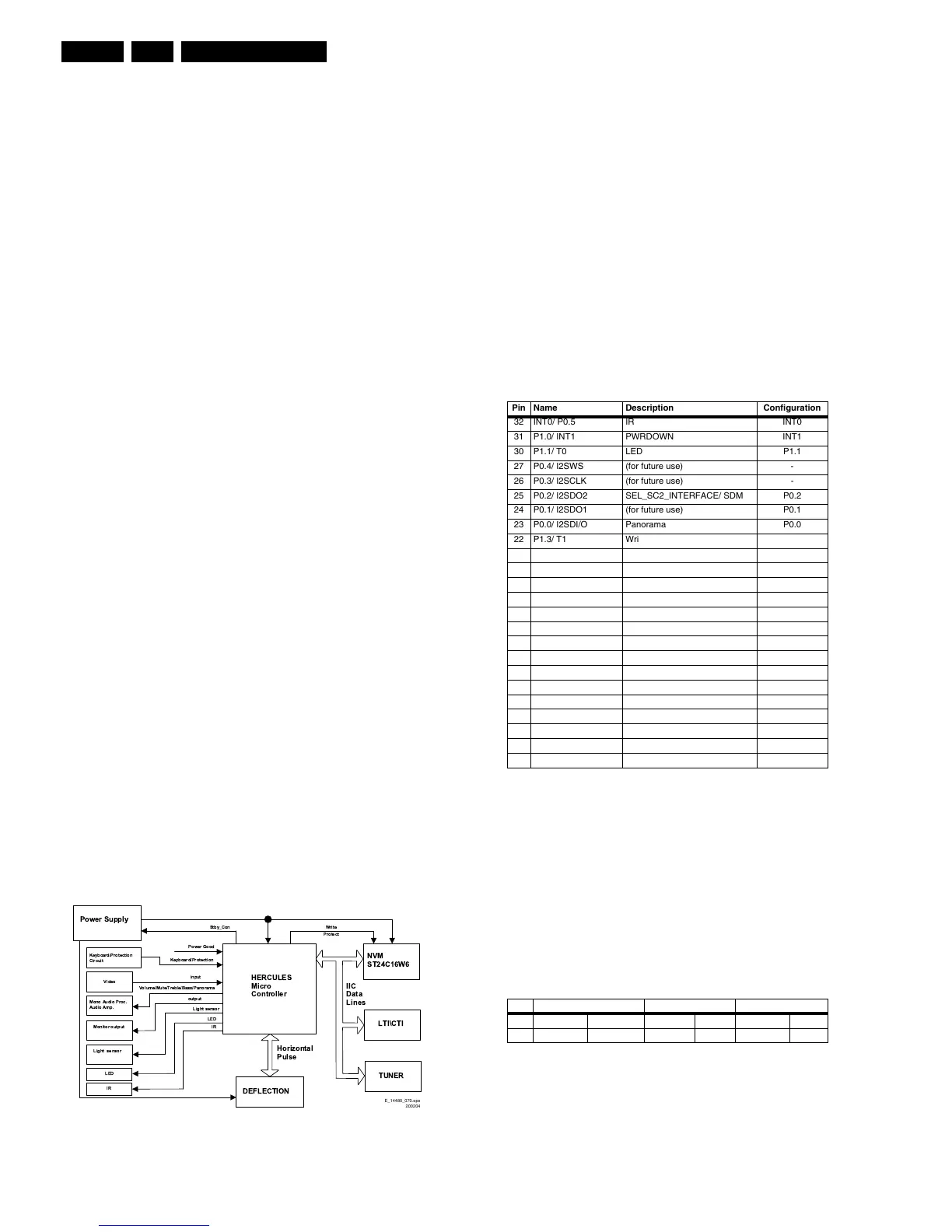
9.4 Control
The Micro Controller is integrated with the Video Processor,
and is called the Hercules. For dynamic data storage, such as
SMART PICTURE and SMART SOUND settings, an external
NVM IC is being used.
Another feature includes an optional Teletext/Closed Caption
decoder with the possibility of different page storage depending
on the Hercules type number.
The Micro Controller ranges in ROM from 128 kB with no TXT-
decoder to 128 kB with a 10 page Teletext or with Closed
Caption.
9.4.1 Block Diagram
The block diagram of the Micro Controller application is shown
below.
Figure 9-4 Micro Controller block diagram
9.4.2 Basic Specification
The Micro Controller operates at the following supply voltages:
• +3.3 V_dc at pins 33, 125, and 19.
• +1.8 V_dc at pins 126, 36, and 33.
• I2C pull up supply: +3.3V_dc.
9.4.3 Pin Configuration and Functionality
The ports of the Micro Controller can be configured as follows:
• A normal input port.
• An input ADC port.
• An output Open Drain port.
• An output Push-Pull port.
• An output PWM port.
• Input/Output Port
The following table shows the ports used for the L04 control:
Table 9-4 Micro Controller ports overview
The description of each functional pin is explained below:
• LED. This signal is used as an indication for the Standby,
Remote and Error Indicator. Region diversity:
– During protection mode, the LED blinks and the set is
in standby mode.
– During error conditions it blinks at a predefined rate.
– After receiving a valid RC-5 or local keyboard
command it flashes once.
– For sets with error message indication, the LED blinks
when message is active and the set is in standby
mode.
Table 9-5 LED signal diversity
• SCL. This is the clock wire of the two-wire single master bi-
directional I2C bus.
• SDA. This is the data wire of the two-wire single master bi-
directional I2C bus.
• STDBY_CON. The Hercules generates this signal. This
can enable the MAIN SMPS in normal operation and
disable it during Standby. It is of logic “low” (0 V) under
normal operation and “high” (3.3 V) during Standby.
!
"
# !$$%
&%'
# ()
*%&)+
)
$!
!
*%&)+
E_14480_070.eps
200204
Pin Name Description Configuration
32 INT0/ P0.5 IR INT0
31 P1.0/ INT1 PWRDOWN INT1
30 P1.1/ T0 LED P1.1
27 P0.4/ I2SWS (for future use) -
26 P0.3/ I2SCLK (for future use) -
25 P0.2/ I2SDO2 SEL_SC2_INTERFACE/ SDM P0.2
24 P0.1/ I2SDO1 (for future use) P0.1
23 P0.0/ I2SDI/O Panorama P0.0
22 P1.3/ T1 Write Protect P1.3
21 P1.6/ SCL SCL SCL
20 P1.7/ SDA SDA SDA
18 P2.0/ TPWM VOL_MUTE P2.0
17 P2.1/ PWM0 ROTATION PWM0
16 P2.2/ PWM1 SEL_LL'/M P2.2
15 P2.3/ PWM2 STANDBY_CON P2.3
14 P3.0/ ADC0 Light Sensor ADC0
13 P3.1/ ADC1 (for future use) -
10 P3.2/ ADC2 (for future use) -
9 P3.3/ ADC3 KEYBOARD ADC3
7 P2.4/ PWM3 A (for future use) P2.4
6 P2.5/ PWM4 B (for future use) P2.5
3 P1.2/ INT2 C (for future use) INT2
2 P1.4/ RX E (for future use) -
1 P1.5/ TX D (for future use) -
LED Europe AP/ LATAM NAFTA
0 LED brighter Standby LED lighted Standby LED lighted Normal
1 LED dimmer Normal LED "off" Normal LED "off" Standby
 Loading...