Do you have a question about the Philips L01.1U and is the answer not in the manual?
Detailed technical parameters and reception capabilities of the TV.
Diagrammatic representation of AV and other input/output connections.
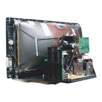
Visual guide to the location of main chassis components and PWB modules.
Critical safety precautions and procedures for performing repairs.
Guidelines for routine maintenance and inspection intervals.
Important warnings regarding high voltage, ESD, and component handling.
General notes and schematic interpretation guidelines for service.
Explanation of front panel controls and basic TV operation.
Guide to operating the TV using top panel controls.
Step-by-step guide for safely disassembling the TV set.
Illustrates two methods for positioning the chassis for service access.
Procedures for removing specific boards and modules from the chassis.
Final checks and steps required before closing the TV set.
Overview of test points on the circuit board assemblies for diagnostics.
Details on entering and using Service Default Alignment Mode (SDAM).
Troubleshooting common picture and sound issues.
Information on using ComPair, a PC-based service tool for diagnostics.
Explanation of how to read and interpret error codes from the buffer.
Method for displaying error codes using the front LED.
Overview of protection modes and error code indications.
Specific tips for diagnosing and repairing common faults.
High-level functional overview of the chassis systems.
Detailed diagrams showing I2C bus connections and supply voltages.
Location and expected waveforms for key test points.
Schematic diagram for the TV's power supply unit.
Circuit diagram for the horizontal deflection system.
Circuit diagram for the vertical deflection system.
Circuit diagram for the tuner and intermediate frequency stages.
Circuit diagram for video and sound intermediate frequency processing.
Circuit diagram for horizontal and vertical synchronization.
Circuit diagram for the main control and microprocessor functions.
Circuit diagram for the audio amplification stage.
Circuit diagram for stereo audio decoding.
Circuit diagram for selecting audio/video input sources.
Circuit diagram for the BTSC NDBX stereo decoder.
Circuit diagram for front panel interfaces and headphone jack.
Circuit diagram for rear panel analog audio/video connections.
Circuit diagrams for PIP and tilt interface functions.
Tables listing component variations based on region and features.
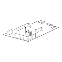
PWB layout illustration for the top side of the mono carrier.
PWB layout overview for the bottom side of the mono carrier.
PWB layout illustration for part 1 of the bottom side.
PWB layout illustration for part 2 of the bottom side.
PWB layout illustration for part 3 of the bottom side.
PWB layout illustration for part 4 of the bottom side.
Circuit diagram for the CRT panel ECO SCAVEM system.
Circuit diagram for the CRT panel ECO SCAVEM system.
PWB layout illustration for the top side of the CRT panel.
PWB layout illustration for the bottom side of the CRT panel.
Circuit diagram for the Side AV and Headphone panel.
PWB layout illustration for the Side AV and Headphone panel.
Circuit diagram for the Slim version of the Side AV/HP panel.
PWB layout for the top side of the Slim Side AV/HP panel.
PWB layout for the bottom side of the Slim Side AV/HP panel.
Circuit diagram for the Wide version of the Side AV/HP panel.
PWB layout for the top side of the Wide Side AV/HP panel.
PWB layout for the bottom side of the Wide Side AV/HP panel.
Circuit diagram for the top control panel interface.
PWB layout for the top side of the top control panel.
PWB layout for the bottom side of the top control panel.
Circuit diagram for the 2D 3-line comb filter for Y/C separation.
PWB layout for the top side of the comb filter.
PWB layout for the bottom side of the comb filter.
Circuit diagram for the top control panel, including voice control.
PWB layout for the top side of the top control panel.
PWB layout for the bottom side of the top control panel.
Circuit diagram for the front interface panel connections.
PWB layout illustration for the front interface panel.
Circuit diagram for DAF and inner pin cushion correction.
PWB layout for the DAF and pin cushion correction circuits.
Prerequisites and general conditions for performing TV alignments.
Procedures for physical adjustments to the TV's hardware.
Step-by-step guide for adjusting the Vg2 voltage for screen brightness.
Procedure for adjusting the focus potentiometer for sharp picture.
Procedures for adjusting TV parameters via software menus.
How to change option bytes to configure features and hardware.
Alignment procedure for the TV tuner, typically after NVM replacement.
Adjustment of red, green, and blue levels for color temperature.
Adjustments for picture size, position, and shape for optimal display.
Alignment procedures for audio settings like AF-M and A2T thresholds.
Overview of the L01.1U AC chassis architecture and features.
Description of mono and stereo audio signal paths.
Detailed explanation of the stereo sound signal processing path.
Detailed explanation of the mono sound signal processing path.
Explanation of the video signal path from RF input to CRT.
Overview of the video signal processing stages.
Description of tuner, IF, and AGC functions.
How the TV selects between different video input sources.
Explanation of comb filter types and their function in Y/C separation.
Description of the color decoder's function for PAL, NTSC, SECAM.
Details on Y/C processing, black/white stretch, and skin tone correction.
Explanation of RGB control for picture parameters and cut-off stabilization.
Description of the RGB amplifier stage driving the CRT.
Explanation of the SCAVEM circuitry for horizontal deflection enhancement.
Description of horizontal and vertical sync signal processing.
Explanation of horizontal and vertical deflection circuits.
Description of the horizontal drive signal generation and EHT protection.
Explanation of the vertical drive circuit and its protection mechanisms.
Details on linearity, S-correction, East/West, and Panorama corrections.
Description of the switching mode power supply and its operation.
Overview of the SMPS and its benefits.
Explanation of Quasi-Resonant mode operation and time intervals.
Description of microprocessor control, I2C bus, and user interface.
Glossary of technical terms and abbreviations used in the manual.