Published by BB 0469 Service PaCE Printed in the Netherlands Subject to modification EN 3122 785 14970
©
Copyright 2004 Philips Consumer Electronics B.V. Eindhoven, The Netherlands.
All rights reserved. No part of this publication may be reproduced, stored in a
retrieval system or transmitted, in any form or by any means, electronic,
mechanical, photocopying, or otherwise without the prior permission of Philips.
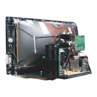
Colour Television Chassis
L04E
AB
E_14970_035.eps
080904
Contents Page Contents Page
1. Technical Specifications, Connections,
and Chassis Overview 2
2. Safety Instructions, Warnings, and Notes 4
3. Directions for Use 6
4. Mechanical Instructions 7
5. Service Modes, Error Codes, and Faultfinding 8
6. Block Diagrams, Testpoint Overviews,
and Waveforms
Wiring Diagram 19
Block Diagram Supply and Deflection 20
Testpoint Overview Mono Carrier 21
Block Diagram IBO Zapper 22
Block Diagram Audio 23
Block Diagram IBO Zapper Panel 24
I2C and Supply Voltage Overview 25
7. Circuit Diagrams and PWB Layouts Diagram PWB
Power Supply (Diagram A1) 26 38-43
Diversity Table for A1 (Power Supply) 27 38-43
Deflection (Diagram A2) 28 38-43
Diversity Table for A2 (Deflection) 29 38-43
Tuner IF (Diagram A3) 30 38-43
Hercules (Diagram A4) 31 38-43
Features & Connectivities (Diagram A5) 32 38-43
Class D - Audio Amplifier (Diagram A6) 33 38-43
Audio Amplifier (Diagram A7) 34 38-43
Rear I/O Scart (Diagram A8) 35 38-43
Front Control (Diagram A9) 36 38-43
DVD Power Supply (Diagram A10)37 38-43
CRT Panel (Diagram B1) 44 46-47
CRT ECO Scavem Panel (Diagram B2) 45 46-47
CRT Interface Panel (Diagram B3) 48 48
Side AV + HP Panel (PV2) (Diagram D) 49 50
Side AV + HP Panel (FL-13) (Diagram D) 51 52
Top Control Panel (PV2) (Diagram E) 53 53
Top Control Panel (FL-13) (Diagram E) 54 54
Linearity & Panorama Panel (Diagram G) 55 55
LTI/CTI PIP Panel (Diagram H) 56 57
Front Interface Panel (FL-13) (Diagram J) 58 58
Front Interface Panel (PV2) (Diagram J) 59 59
Front Interface and Keyb. Panel (Diagram J) 60 61
IBO Zapper Panel: MOJO (Diagram K1) 62 69-70
IBO Zapper Panel: Flash Memory (Diagram K2) 63 69-70
IBO Zapper Panel: Power Supply (Diagram K3) 64 69-70
IBO Zapper Panel: Interface (Diagram K4) 65 69-70
IBO Zapper Panel: Analog Back End(Diagr. K5) 66 69-70
IBO Zapper Panel: Front End (Diagram K6) 67 69-70
IBO Zapper Panel: Common Interface(Diagr. K7)68 69-70
8. Alignments 71
9. Circuit Descriptions 79
Abbreviation List 81
IC Data Sheets 83
10 Spare Parts List 85
11 Revision List 91