Interconnectivity
Page 10 of 14
PDIUSBD12 Evaluation Board (PC Kit) User’s Manual REV. 2.1
_______________________________________________________________________________________________
Philips Semiconductors - Asia Product Innovation Centre
Visit http://www.flexiusb.com
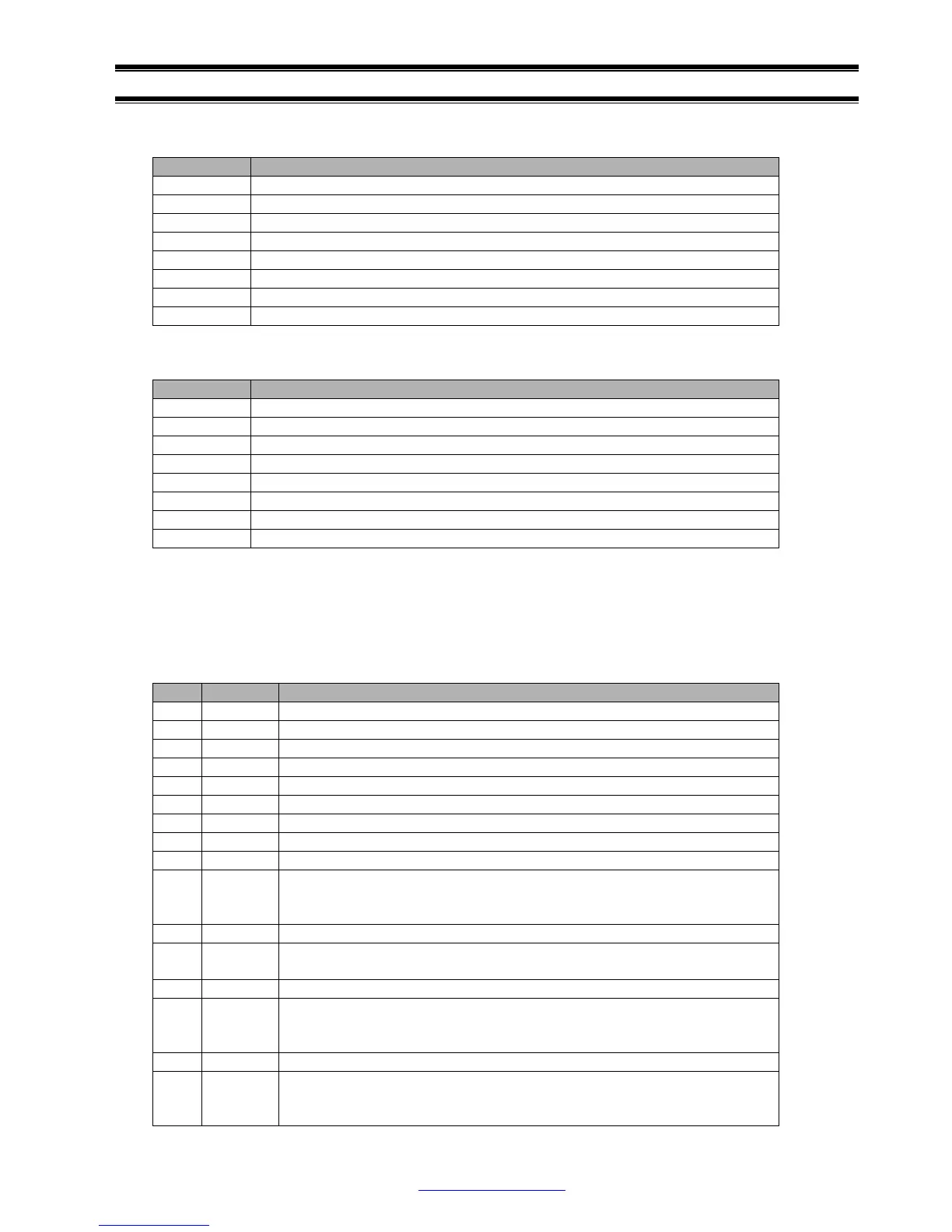
Bit description for general input port:
Bit Usage
0 Key S1, ‘0’ for pressed
1 Key S2, ‘0’ for pressed
2 Key S3, ‘0’ for pressed
3 Key S4, ‘0’ for pressed
4
D12 GoodLink
TM
pin state
5 USB bus power state, ‘1’ for USB VBUS present
6 D12 SUSPEND pin state
7 D12 INT_N pin state
Bit description for general output port:
Bit Usage
0 LED D2, ‘1’ lights up LED
1 LED D3, ‘1’ lights up LED
2 LED D4, ‘1’ lights up LED
3 LED D5, ‘1’ lights up LED
4 Reserved
5 Reserved
6 Suspend control, ‘1’ forces D12 SUSPEND pin low
7 Interrupt enable, ‘1’ enables interrupt
Connectors
25 wire connector for PDIUSBD12 evaluation board:
Pin Type Description
1 POWER VCC
2 POWER GND
3 I/O DATA7
4 I/O Zero Wait State
5 I/O DATA6
6 I/O Reserved
7 I/O DATA5
8 O CLKOUT: This line is connected to PDIUSBD12 CLKOUT pin.
9 I/O DATA4
10 I -AD_EN: This line is the decoder output for address decoding A3 to
A9. This signal is active low when PDIUSBD12 evaluation board I/O
address is selected.
11 I/O DATA3
12 I RESET: This line is used to reset or initialize system logic upon
power-up and is active high.
13 I/O DATA2
14 I -IOW: This command line instructs an I/O device to read the data on
the data bus. It may be driven by the processor or the DMA controller.
This signal is active low.
15 I/O DATA1
16 I -IOR: This command line instructs an I/O device to drive its data onto
the data bus. It may be driven by the processor or the DMA controller.
This signal is active low.