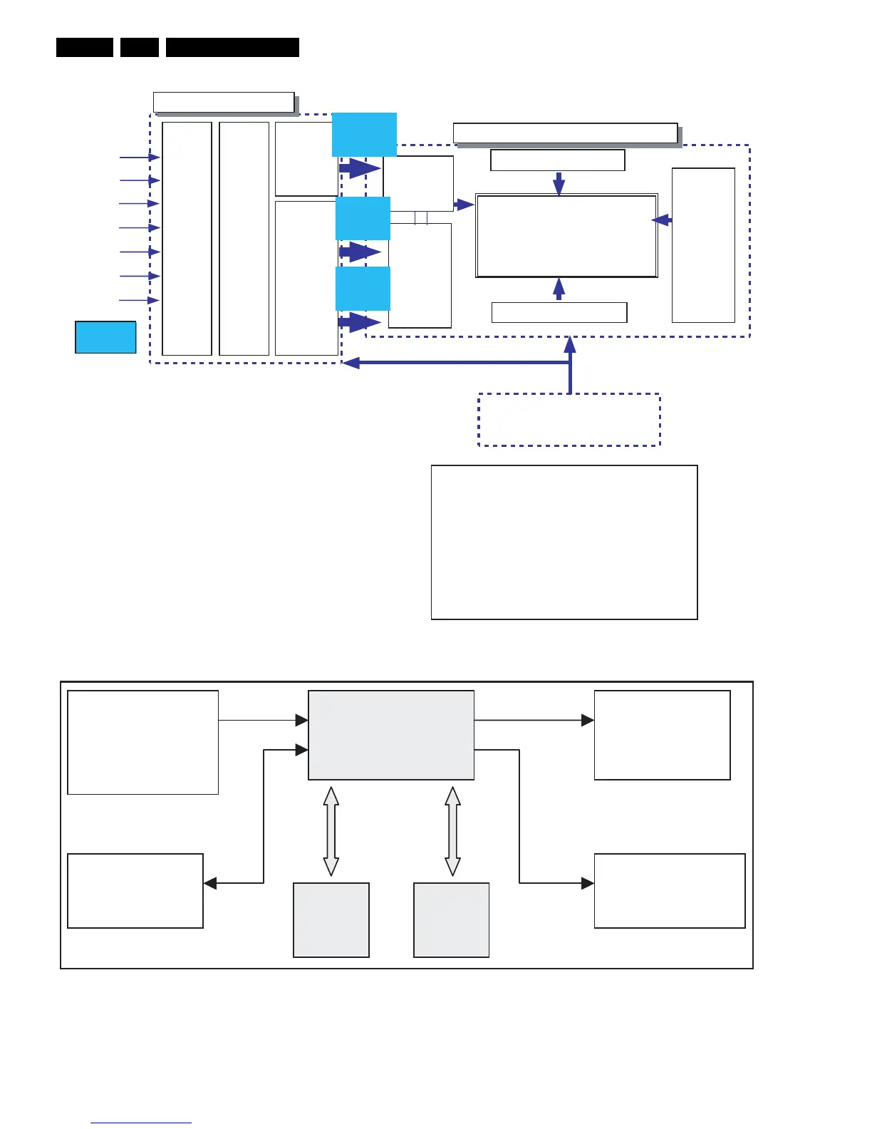
Block Diagrams, Test Point Overview, and Waveforms
EN 42 SDI PDP6.
Figure 6-5 Block diagram (42" HD v3)
Figure 6-6 Block diagram (42" HD v4)
1024× 768 Pixels
1024× 3× 768 Cells
YPulse
Generator
Row
Driver
VsVa
Vcc
Vsync
Enable
Hsync
DCLK
DRAM
Display
Data
Driver
Timing Controller
Driver
Timing
Scan
Timing
Vdd
DATA_R
8Bits
Column Driver
LOGIC CONTROL
DRIVER CIRCUIT & PANEL
DATA_G
8Bits
DATA_B
8Bits
Input Data Processor
Data Controller
XPulse
Generator
Vset Vsc
Ve
LVDS
Interface
Column Driver
- Vcc : Voltage for Logic Control
- Vdd : Voltage for Fet driver
- Va : Voltage for address pulse
- Vs : Voltage sustain pulse
- Vsc : Voltage for scan pulse
- Ve : Voltage for X ramp pulse
- Vset : Voltage for Y ramp pulse
Reference
F_14991_018.eps
030805
ASIC
SPS-NIRB_ 816P
LVDS Input
(DCLK, RG B data,
V/Hsync
X,Y main
Control
128M
DDR
128M
DDR
TCP
CLK, Data control
I2C Interface
Signal
 Loading...