Version: 13. September 2004
35
Section 11, Transmitter driver and PA
[ ] P1 100R 0,5W Cermet lying RM 5x10mm F/G3
The following transistors may easy be damaged by ESD. Dont
forget to discharge yourself, use a potential free soldering
station.
Bend leads of BRF96 away from the marking text.
[ ] T3 BFR96(S) G4
[ ] C53 47nF 473 G4
[ ] C54 100nF 104 G4
[ ] C56 47nF 473 H4
[ ] C57 47nF 473 G4
[ ] C58 47nF 473 H4
[ ] C60 2,2nF 222 H3
[ ] C61 47nF 473 F4
[ ] C62 47nF 473 F3
[ ] C63 47nF 473 G3
[ ] C65 47nF 473 H1
[ ] C66 100nF 104 H3
[ ] C68 100nF 104 H2/3
[ ] C69 100nF 104 H2
[ ] C72 47nF 473 F1
[ ] C64 0,47µF Film RM 5mm G3
[ ] C55 0,1µF Film RM 5mm G3
[ ] C70 1µF Film RM 5mm H2
[ ] C67 47µF/16V radial G3
[ ] C71 100µF/25V radial H1
[ ] D3 BA479 F4
[ ] Dr6 47µH SMCC F3/4
[ ] Dr7 10µH SMCC G3
[ ] R34 1K F4
[ ] R35 2k7 G4
[ ] R36 1k2 G4
[ x] R37 10R SMD G4
[ ] R38 39R G4
[ ] R39 68R H4
[ ] R40 820R (adjust for Iquiesc. T5~ 100mA) H4
[x ] R41 4,7R SMD H4
[x ] R42 4,7R SMD H3
[x ] R43 1R SMD H3
[ ] R44 270R 1 Watt Metal film G4
[ ] R45 5,6R H1/2
[ ] R46 10R G/H3
[ ] R47 10R H3
[X] R48 1R SMD 1206 H2
[X] R49 1R SMD 1206 H2
[X] R50 1R SMD 1206 H2
[X] R51 1R SMD 1206 H2
Mount the TO220 transistors, so they are flush with the pc
board edge. Later they will be mounted on the back of the box.
[ ] T4 BD242/ BD244 H4
[ ] T5 2SC1970 Mitsubishi!! H3/4
[ ] T6 2SC1969 Mitsubishi!! H2
[ ] T7 2SC1969 Mitsubishi!! H3
[ ] T8 BD242/ BD244 H1/2
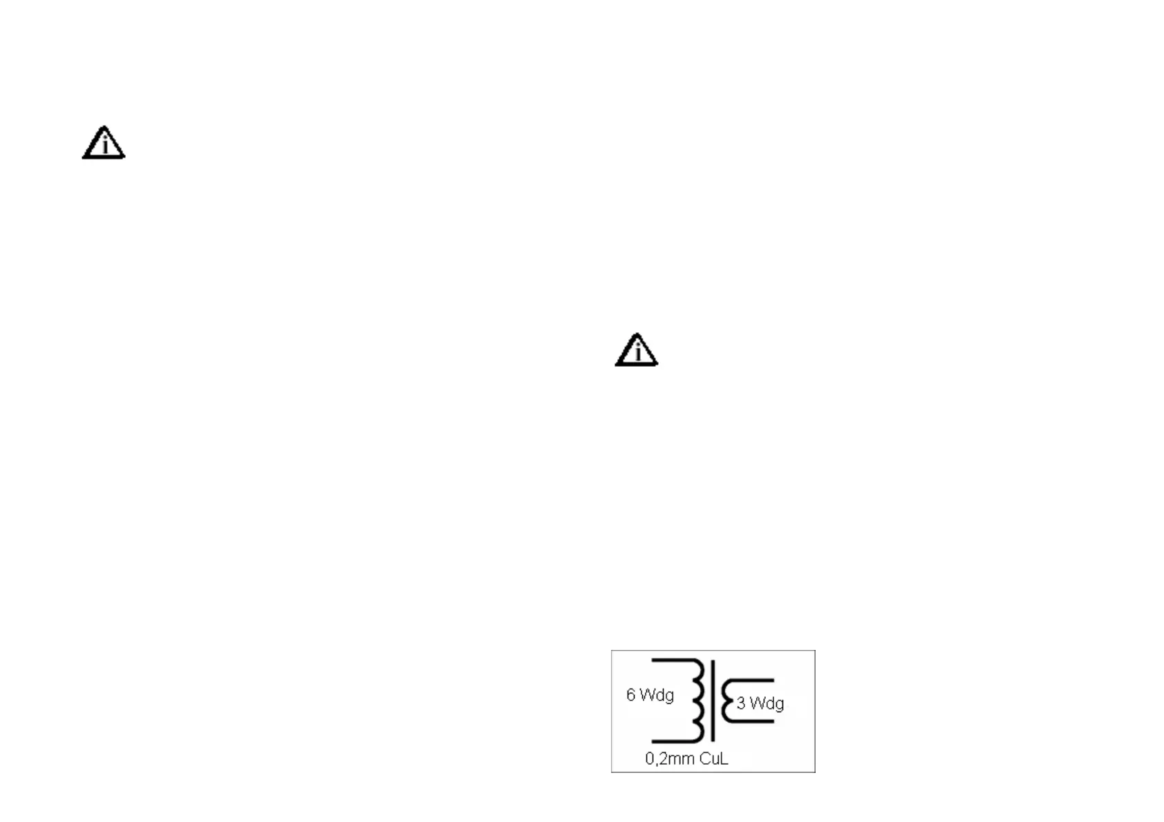
We continue with the broad band transformers Tr3 and Tr4. They are identi-
cal. These transformers are wound on pig nose cores.
Building instruction Tr3:
Put the pig nose in front of you, pointing the holes from left to right, an
mark the left side with a drop of colour (Nail lacquer is good, felt tipped
pens works badly). The marking is important
to avoid mixing up primary and secondary.
Tr3 contains a primary of 6 turns and a
secondary of 3 turns. As in most other
transformer diagrams, one winding is mar-
ked with a dot. This is always the beginning
of the winding.